
User manual

R
SNS
(W)
I
LED
(mA)
400
370
340
310
280
250
220
190
160
P
OUT
(W)
9.8
9.1
8.3
7.6
6.8
6.1
5.3
4.6
2.62.52.42.32.22.12.01.91.81.71.61.51.41.3
3.8
R
SNS
(W)
I
LED
(mA)
270
250
230
210
190
170
150
130
110
P
OUT
(W)
9.8
9.1
8.3
7.6
6.8
6.1
5.3
4.6
2.62.52.42.32.22.12.01.91.81.71.61.51.41.3
3.8
R
SNS
(W)
I
LED
(mA)
322
298
274
250
226
202
178
154
130
P
OUT
(W)
9.8
9.1
8.3
7.6
6.8
6.1
5.3
4.6
2.62.52.42.32.22.12.01.91.81.71.61.51.41.3
3.8
Design Guide
www.ti.com
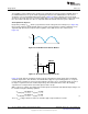
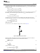
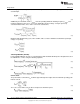
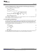
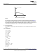
Output Power and Current Sense Resistor
Due to the interaction of the AC-coupled line-injection voltage with the FLTR2 signal, the equations for
determining the correct sense resistor R
SNS
(shown as R14 in the evaluation board schematic) for a
desired output power P
OUT
are complex and beyond the scope of this document. Instead, performance
graphs showing the relationship between LED current, P
OUT
and R
SNS
are shown in Figure 29, Figure 30
and Figure 31 for common stack voltages of 8, 10 and 12 LEDs. By referring to these graphs, users can
choose R14 values that will meet their LED current and output power requirements.
Figure 29. I
LED
vs. P
OUT
vs. R
SNS
Figure 30. I
LED
vs. P
OUT
vs. R
SNS
for 12 LEDs (V
f
=3.0V) for 10 LEDs (V
f
=3.0V)
Figure 31. I
LED
vs. P
OUT
vs. R
SNS
for 8 LEDs (V
f
=3.0V)
Inductor
Peak inductor currents will need to be calculated as shown below based on the V
FLTR2
voltages and chosen
sense resistor R14 at the maximum and minimum peak input voltages,
(5)
14
AN-2127 LM3448 A19 Edison Retrofit Evaluation Board SNOA559B–October 2011–Revised May 2013
Submit Documentation Feedback
Copyright © 2011–2013, Texas Instruments Incorporated