
User manual

R
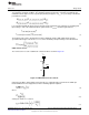
FLTR1
R
SNS
PWM
I-LIM
1.27V
ISNS
ASNS
GND
FLTR1
FLTR2
DIM
DIM DECODER
4.9V
Tri-State
50k
370k
C
FLTR2
C
FLTR1
1k
RAMP GEN.
5.9 kHz
3V
1V
750 mV
125 ns
LEADING EDGE BLANKING
1V
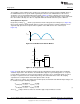
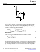
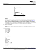
The PWM reference increases
as the line voltage increases.
As line voltage increases, the voltage across the
inductor increases, and the peak current increases.
LED Current
RAMP
www.ti.com
Design Guide
Figure 28. Typical Operation of FLTR2 Pin
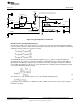
Off-time, On-time and Switching Frequency
The AC mains voltage at the line frequency f
L
is assumed to be perfectly sinusoidal and the diode bridge
ideal. This yields a perfect rectified sinusoid at the input to the buck converter. The maximum, nominal and
minimum peak input voltages are defined as follows,
(2)
The LM3448 will operate as a constant off-time regulator, and so t
OFF
will be constant throughout all
operating points. The on-time t
ON
(and subsequently the switching frequency f
SW
) will vary depending on
input voltage and LED stack voltage values. For this buck converter operating in continuous conduction
mode (CCM), the minimum on-time t
ON(MIN)
can be determined for a maximum desired switching frequency
f
SW(MAX)
at the maximum peak input voltage,
(3)
The off-time t
OFF
is now calculated where T
S(MIN)
is the minimum switching period,
(4)
It is important to note that there is a minimum on-time of 200ns that needs to be met in order for proper
LED driver operation.
13
SNOA559B–October 2011–Revised May 2013 AN-2127 LM3448 A19 Edison Retrofit Evaluation Board
Submit Documentation Feedback
Copyright © 2011–2013, Texas Instruments Incorporated