User's Guide SNOA559B – October 2011 – Revised May 2013 AN-2127 LM3448 A19 Edison Retrofit Evaluation Board 1 Introduction This demonstration board highlights the performance of a LM3448 non-isolated LED driver solution that can be used to power a single LED string consisting of eight to twelve series connected LEDs from a 85 VRMS to 135 VRMS, 60 Hz input power supply. This is a two-layer board using the bottom and top layer for component placement.
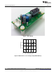
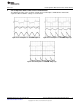
Performance Specifications www.ti.com Figure 1. Demo Board LED CURRENT (mA) 200 150 100 50 0 20 40 60 80 100 INPUT VOLTAGE (VRMS) 120 Figure 2. LED Current vs.
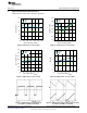
Typical Performance Characteristics www.ti.com 5 Typical Performance Characteristics TJ=25°C and VCC=12V, unless otherwise specified. 84 0.90 12 LEDs 10 LEDs 8 LEDs 0.88 POWER FACTOR EFFICIENCY (%) 82 80 78 12 LEDs 10 LEDs 8 LEDs 0.86 0.84 0.82 76 0.80 74 80 90 100 110 120 130 INPUT VOLTAGE (VRMS) Figure 3. Efficiency vs. Line Voltage 350 90 100 110 120 130 INPUT VOLTAGE VRMS 140 Figure 4. Power Factor vs.
EMI Performance 6 www.ti.com EMI Performance 120V, 6.5W Conducted EMI Scans 4 Figure 9. LINE – CISPR/FCC Class B Peak Scan Figure 10. NEUTRAL – CISPR/FCC Class B Peak Scan Figure 11. LINE – CISPR/FCC Class B Average Scan Figure 12.
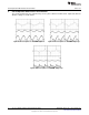
Circuit Operation With Forward Phase TRIAC Dimmer www.ti.com 7 Circuit Operation With Forward Phase TRIAC Dimmer The dimming operation of the circuit was verified using a forward phase TRIAC dimmer. Waveforms captured at different dimmer settings are shown below: Figure 13. Forward phase circuit at full brightness Figure 14. Forward phase circuit at 90° firing angle Figure 15.
Circuit Operation With Reverse Phase Dimmer 8 www.ti.com Circuit Operation With Reverse Phase Dimmer The circuit operation was also verified using a reverse phase dimmer and waveforms captured at different dimmer settings are shown below: Figure 16. Reverse phase circuit at full brightness Figure 17. Reverse phase circuit at 90° firing angle Figure 18.
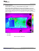
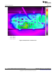
Thermal Performance www.ti.com 9 Thermal Performance The board temperature was measured using an IR camera (HIS-3000, Wahl) while running under the following conditions: VIN = 120VRMS, ILED = 181mA, # of LEDs = 12, POUT = 6.5W. NOTE: Thermal performance is highly dependent on the user's final end-application enclosure, heatsinking methods, ambient operating temperature, and PCB board layout in addition to the electrical operating conditions. This LM3448 evaluation board is optimized to supply 6.
Thermal Performance • • • • Cursor Cursor Cursor Cursor www.ti.com 1: 68.1°C 2: 64.7°C 3: 62.6°C 4: 61.7°C Figure 20.
LM3448 Device Pin-Out www.ti.com 10 LM3448 Device Pin-Out SW 1 16 SW SW 2 15 SW NC 3 14 NC BLDR 4 13 ISNS GND 5 12 GND VCC 6 11 FLTR2 ASNS 7 10 COFF FLTR1 8 9 DIM Figure 21. Device Pin-Out Table 1. Pin Description 16 Pin Narrow SOIC Pin # Name 1, 2, 15, 16 SW Description Drain connection of internal 600V MOSFET. 3, 14 NC No connect. Provides clearance between high voltage and low voltage pins. Do not tie to GND. 4 BLDR Bleeder pin.
Demo Board Wiring Overview Demo Board Wiring Overview LED - TP4 LED + TP3 TP1 LINE J5 J10 11 www.ti.com TP2 NEUTRAL Figure 22. Wiring Connection Diagram Table 2. Test Points 12 Test Point Name I/O Description TP3 LED + Output LED Constant Current Supply Supplies voltage and constant-current to anode of LED string. TP4 LED - Output LED Return Connection (not GND) Connects to cathode of LED string. Do NOT connect to GND.
Design Guide www.ti.com Figure 24. Bottom View 13 Design Guide D1 V+ V+ R1 R2 C1 D2 C10 R3 R7 C6 Q1 C16 VLED+ R4 R22 C5 D8 VCC D7 D4 C4 + C3 C8 R8 C2 L1 VLED± L2 L3 C13 R5 R6 LM3448 LINE 9 DIM NEUTRAL FLTR1 8 R9 COFF LINE EMI FILTER 10 COFF ASNS 7 VCC C14 R15 C15 11 FLTR2 VCC 6 12 GND GND 5 13 ISNS BLDR 4 R16 COFF R14 14 NC NC 3 15 SW SW 2 16 SW SW 1 U1 C12 COFF Current Source Figure 25.
Design Guide www.ti.com 13.1 Buck Converter The following section explains how to design a non-isolated buck converter using the LM3448. Refer to the LM3448 datasheet for specific details regarding the function of the LM3448 device. All reference designators refer to the Evaluation Board Schematic in Figure 25 unless otherwise noted. The circuit operates in open-loop based on a constant off-time that is set by selecting appropriate circuit components.
Design Guide www.ti.com 750 mV 50k DIM DECODER ASNS As line voltage increases, the voltage across the inductor increases, and the peak current increases. 370k Tri-State 4.9V RFLTR1 PWM I-LIM FLTR1 RAMP LED Current 1.27V CFLTR1 RAMP GEN. 5.9 kHz 3V 1V 1k ISNS 1V RSNS DIM LEADING EDGE BLANKING FLTR2 The PWM reference increases as the line voltage increases. GND 125 ns CFLTR2 Figure 28.
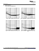
Design Guide www.ti.com Output Power and Current Sense Resistor 322 9.8 250 9.1 298 9.1 230 8.3 274 8.3 210 7.6 250 7.6 190 6.8 226 6.8 170 6.1 202 6.1 150 5.3 178 5.3 130 4.6 154 4.6 3.8 130 110 1.3 1.4 1.5 1.6 1.7 1.8 1.9 2.0 POUT (W) 9.
Design Guide www.ti.com Inductor ripple current will need to be specified by the user based on desired EMI performance, inductor size and other operating conditions. The following equations show how to calculate for maximum and minimum inductor ripple currents respectively by basing the ripple (i.e.
Design Guide www.ti.com Re-arranging the above equation results in R16 being calculated where C12 is typically chosen as value around 470pF, (12) Additionally, the maximum on-time tON(MAX) and corresponding minimum switching frequency fSW(MIN) and maximum switching period TS(MAX) occur at the minimum peak input voltage.
Design Guide www.ti.com Re-circulating Diode The main re-circulating diode (D4) should be sized to block the maximum reverse voltage VRD4(MAX), operate at the maximum peak IDR-PK(MAX) and RMS currents ID4-RMS(MAX), and dissipate the maximum power PD4(MAX) as determined by the following equations, (20) (21) (22) (23) NOTE: For proper converter operation, the chosen diode should have a reverse recovery time that is less than the LM3448's leading edge blanking time of 125ns. 13.
Design Guide www.ti.com V+ R1 R3 Q1 VCC R22 D8 D7 C8 R8 LM3448 VCC 6 Figure 33. Bias Supply Circuit Input Capacitance The input capacitors C1 and C10 have to be able to provide energy during the worst-case switching period at the peak of the AC voltage input. They should be high frequency, high stability capacitors (usually metallized film capacitors, either polypropylene or polyester) with an AC voltage rating equal to the maximum input voltage.
Design Guide www.ti.com LINE R5 L1 C5 C16 C6 D2 C2 V+ R4 NEUTRAL R6 L2 Figure 34. Input EMI Filter Conducted Figure 34 shows a typical filter used with this LM3448 flyback design. In order to conform to conducted standards, a fourth order filter is implemented using inductors and "X" rated AC capacitors. If sized properly, this filter design can provide ample attenuation of the switching frequency and lower order harmonics contributing to differential noise.
Design Calculations www.ti.com Triac Fires Æ Inrush Spike Iin(t) 0 t Potential Misfire Figure 35. Inrush Current Spike Damper The inrush spike can also excite a resonance between the input filter of the TRIAC and the input filter of the converter. The associated interaction can cause the current to ring negative, as shown in Figure 35, thereby shutting off the TRIAC.
Design Calculations www.ti.com VZ(D7)=12V R8=49.9kΩ VGS(Q1)=0.7V 14.2 Preliminary Calculations Nominal peak input voltage: (29) Calculate minimum on-time and verify it's greater than 200ns: (30) Calculate off-time: (31) From Figure 29, choose R14=2.0Ω for 6.5W output power with 12 LEDs. 14.3 FLTR2 AC-LINE Injection Choose VINJECT(NOM)=1.0V Choose R2=R7=274kΩ Calculate R15: (32) or, (33) Calculate maximum FLTR2 pin voltage and verify it is less than 1.
Design Calculations www.ti.com 14.4 Inductor Calculate peak inductor currents at the minimum and maximum peak input voltages: (36) Calculate inductor ripple currents at the minimum and maximum peak input voltages based on 80% of maximum peak inductor currents: (37) Verify that converter is in CCM operation at the minimum peak input voltage: (38) Calculate inductor value: (39) 14.5 COFF Current Source Choose capacitor C12=470pF.
Design Calculations www.ti.com 14.6 SW FET Calculate maximum peak SW FET current: (43) Calculate maximum RMS SW FET current: (44) Calculate maximum power dissipation: (45) 14.7 Current Limit Calculate peak inductor current limit: (46) Power dissipation: (47) Resulting component choice: (48) 14.
Design Calculations www.ti.com 14.9 PassFET Calculate maximum peak voltage: (54) Calculate current: (55) Calculate maximum power dissipation: (56) Resulting component choice: (57) 14.10 Input Capacitance Minimum capacitance: (58) AC Voltage rating: (59) DC Voltage rating: (60) Resulting component choice: (61) 14.
Evaluation Board Schematic www.ti.
Bill of Materials 16 26 www.ti.com Bill of Materials Part ID Description Manufacturer Part Number C1, C10 CAP CER 47000PF 500V X7R 1210 Johanson Dielectrics 501S41W473KV4E C2, C6 CAP FILM MKP .015UF 310VAC X2 Vishay/BC Comp BFC233820153 C3 CAP 470UF 50V ELECT PW RADIAL Nichicon UPW1H471MHD C4 DNP DNP DNP C5, C16 CAP CER .
PCB Layout www.ti.com 17 PCB Layout NOTE: Spacing between traces and components of this evaluation board are based on high voltage recommendations for designs that will be potted. Users are cautioned to satisfy themselves as to the suitability of this design for the intended end application and take any necessary precautions where high voltage layout and spacing rules must be followed. Figure 36. Top Layer Figure 37.
IMPORTANT NOTICE Texas Instruments Incorporated and its subsidiaries (TI) reserve the right to make corrections, enhancements, improvements and other changes to its semiconductor products and services per JESD46, latest issue, and to discontinue any product or service per JESD48, latest issue. Buyers should obtain the latest relevant information before placing orders and should verify that such information is current and complete.