
User manual

1
4
3
2
10
7
8
9
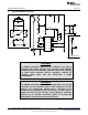
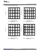
I
SNS
FLTR1
GATE
BLDR
COFF
V
CC
ASNS
DIM
5 6FLTR2 GND
www.ti.com
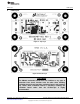
Pin-Out
4 Pin-Out
Figure 1. 10-Pin VSSOP
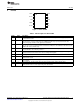
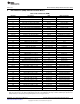
Table 1. Pin Description 10 Pin VSSOP
Pin No Name Description
1 ASNS PWM output of the triac dim decoder circuit. Outputs a 0 to 4V PWM signal with a duty cycle proportional to
the triac dimmer on-time.
2 FLTR1 First filter input. The 120Hz PWM signal from ASNS is filtered to a DC signal and compared to a 1 to 3V,
5.85 kHz ramp to generate a higher frequency PWM signal with a duty cycle proportional to the triac
dimmer firing angle. Pull above 4.9V (typical) to tri-state DIM.
3 DIM Input/output dual function dim pin. This pin can be driven with an external PWM signal to dim the LEDs. It
may also be used as an output signal and connected to the DIM pin of other LM3445 or LED drivers to dim
multiple LED circuits simultaneously.
4 COFF OFF time setting pin. A user set current and capacitor connected from the output to this pin sets the
constant OFF time of the switching controller.
5 FLTR2 Second filter input. A capacitor tied to this pin filters the PWM dimming signal to supply a DC voltage to
control the LED current. Could also be used as an analog dimming input.
6 GND Circuit ground connection.
7 ISNS LED current sense pin. Connect a resistor from main switching MOSFET source, ISNS to GND to set the
maximum LED current.
8 GATE Power MOSFET driver pin. This output provides the gate drive for the power switching MOSFET of the
buck controller.
9 V
CC
Input voltage pin. This pin provides the power for the internal control circuitry and gate driver.
10 BLDR Bleeder pin. Provides the input signal to the angle detect circuitry as well as a current path through a
switched 230Ω resistor to ensure proper firing of the triac dimmer.
3
SNVA442C–June 2010–Revised May 2013 AN-2061 LM3445 A19 Edison Retrofit Evaluation Board
Submit Documentation Feedback
Copyright © 2010–2013, Texas Instruments Incorporated