
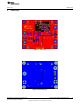
User manual

D1 o 12A, 100V, DPAK
mW600mV600A1VIP
FDDD
=
x
=
x
=
A1II
LEDMAXD
==
-
V5.31VV
OMAXRD
==
-
Q1 o 40A, 100V, DPAK
mW20m50mA640RIP
2
DSON
2
RMSTT
=
:x
=
x
=
-
x
I
RMST
=
-
I
LED
D
c
=
x
mA640
=
0.238
A1
762.0
D
=
A2.2A1
=
x
683.01-
683.0
I
MAXT-
V5.31VV
OMAXT
==
-
C2 = C3 = C16 = C18
= 4.7 PF
mA72
mA250
==
I
RMSIN
=
-
'i
PP-L
12 12
C
IN
==
kHz700mV100 x
250 mA
F0.45 P=
f
'v
SWPPIN-
x
'i
PP-L
x8 x8
F1.0C12 P=
F1.0C8 P=
:10R20 =
www.ti.com
Design Procedure
(32)
6.9 Input Capacitance
Solve for the minimum C
IN
:
(33)
To minimize power supply interaction a much larger capacitance of approximately 20 µF is used, therefore
the actual Δv
IN-PP
is much lower. Since high voltage ceramic capacitor selection is limited, four 4.7 µF X7R
capacitors are chosen.
Determine minimum allowable RMS current rating:
(34)
The chosen components from step 8 are:
(35)
6.10 NFET
Determine minimum Q1 voltage rating and current rating:
(36)
(37)
A 100V NFET is chosen with a current rating of 40A due to the low R
DS-ON
= 50 mΩ. Determine I
T-RMS
and
P
T
:
(38)
(39)
The chosen component from step 9 is:
(40)
6.11 Diode
Determine minimum D1 voltage rating and current rating:
(41)
(42)
A 100V diode is chosen with a current rating of 12A and V
D
= 600 mV. Determine P
D
:
(43)
The chosen component from step 10 is:
(44)
6.12 Input UVLO
Since PWM dimming will be evaluated a three resistor network will be used. Assume R13 = 10 kΩ and
solve for R5:
9
SNVA404B–July 2009–Revised May 2013 AN-1986 LM3429 Boost Evaluation Board
Submit Documentation Feedback
Copyright © 2009–2013, Texas Instruments Incorporated