
User manual

www.ti.com
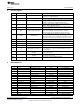
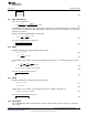
Pin Descriptions
3 Pin Descriptions
Pin Name Description Application Information
Bypass with 100 nF capacitor to AGND as close to the device as
1 V
IN
Input Voltage
possible in the circuit board layout.
2 COMP Compensation Connect a capacitor to AGND.
Connect a resistor to AGND to set the signal current. For analog
3 CSH Current Sense High dimming, connect a controlled current source or a potentiometer
to AGND as detailed in the Analog Dimming section.
Connect a resistor from the switch node and a capacitor to
4 RCT Resistor Capacitor Timing
AGND to set the switching frequency.
Connect to PGND through the DAP copper circuit board pad to
5 AGND Analog Ground
provide proper ground return for CSH, COMP, and RCT.
Connect to a resistor divider from V
O
to program output over-
6 OVP Over-Voltage Protection voltage lockout (OVLO). Turn-off threshold is 1.24V and
hysteresis for turn-on is provided by 20 µA current source.
Connect a PWM signal for dimming as detailed in the PWM
Dimming section and/or a resistor divider from V
IN
to program
7 nDIM Not DIM input
input under-voltage lockout (UVLO). Turn-on threshold is 1.24V
and hysteresis for turn-off is provided by 20 µA current source.
8 NC No Connection Leave open.
Connect to AGND through the DAP copper circuit board pad to
9 PGND Power Ground
provide proper ground return for GATE.
10 GATE Gate Drive Output Connect to the gate of the external NFET.
11 V
CC
Internal Regulator Output Bypass with a 2.2 µF–3.3 µF, ceramic capacitor to PGND.
Connect to the drain of the main N-channel MosFET switch for
12 IS Main Switch Current Sense R
DS-ON
sensing or to a sense resistor installed in the source of
the same device.
High-Side LED Current Sense Connect through a series resistor to the positive side of the LED
13 HSP
Positive current sense resistor.
High-Side LED Current Sense Connect through a series resistor to the negative side of the
14 HSN
Negative LED current sense resistor.
DAP Star ground, connecting AGND and PGND.
DAP Thermal pad on bottom of IC
(15)
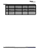
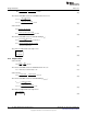
4 Bill of Materials
Qty Part ID Part Value Manufacturer Part Number
2 C1, C4 0.1 µF X7R 10% 100V TDK C2012X7R2A104K
4 C2, C3, C16, C18 4.7 µF X7R 10% 100V MURATA GRM55ER72A475KA01L
3 C6, C17, C19 2.2 µF X7R 10% 100V TDK C4532X7R2A225K
1 C7 1000 pF COG/NPO 5% 50V MURATA GRM2165C1H102JA01D
1 C8 1 µF X7R 10% 16V MURATA GRM21BR71C105KA01L
1 C9 2.2 µF X7R 10% 16V MURATA GRM21BR71C225KA12L
1 C12 0.1 µF X7R 10% 25V MURATA GRM21BR71E104KA01L
1 D1 Schottky 100V 12A VISHAY 12CWQ10FNPBF
4 J1, J2, J4, J5 banana jack KEYSTONE 575-8
1 J7 2 x 7 shrouded header SAMTEC TSSH-107-01-SDRA
1 L1 33 µH 20% 6.3A COILCRAFT MSS1278-333MLB
1 Q1 NMOS 100V 40A VISHAY SUD40N10-25
1 Q3 NMOS 60V 260 mA ON-SEMI 2N7002ET1G
1 R1 12.4 kΩ 1% VISHAY CRCW080512k4FKEA
1 R2 0Ω 1% VISHAY CRCW08050000Z0EA
2 R3, R20 10Ω 1% VISHAY CRCW080510R0FKEA
3
SNVA404B–July 2009–Revised May 2013 AN-1986 LM3429 Boost Evaluation Board
Submit Documentation Feedback
Copyright © 2009–2013, Texas Instruments Incorporated