
User manual

www.ti.com
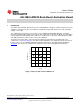
Pin Descriptions
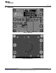
3 Pin Descriptions
Pin Name Description Application Information
Bypass with 100 nF capacitor to AGND as close to the device as
1 V
IN
Input Voltage
possible in the circuit board layout.
2 COMP Compensation Connect a capacitor to AGND.
Connect a resistor to AGND to set the signal current. For analog
3 CSH Current Sense High dimming, connect a controlled current source or a potentiometer
to AGND as detailed in the Analog Dimming section.
Connect a resistor from the switch node and a capacitor to
4 RCT Resistor Capacitor Timing
AGND to set the switching frequency.
Connect to PGND through the DAP copper circuit board pad to
5 AGND Analog Ground
provide proper ground return for CSH, COMP, and RCT.
Connect to a resistor divider from V
O
to program output over-
6 OVP Over-Voltage Protection voltage lockout (OVLO). Turn-off threshold is 1.24V and
hysteresis for turn-on is provided by 20 µA current source.
Connect a PWM signal for dimming as detailed in the PWM
Dimming section and/or a resistor divider from V
IN
to program
7 nDIM Not DIM input
input under-voltage lockout (UVLO). Turn-on threshold is 1.24V
and hysteresis for turn-off is provided by 20 µA current source.
8 NC No Connection Leave open.
Connect to AGND through the DAP copper circuit board pad to
9 PGND Power Ground
provide proper ground return for GATE.
10 GATE Gate Drive Output Connect to the gate of the external NFET.
11 V
CC
Internal Regulator Output Bypass with a 2.2 µF–3.3 µF, ceramic capacitor to PGND.
Connect to the drain of the main N-channel MosFET switch for
12 IS Main Switch Current Sense R
DS-ON
sensing or to a sense resistor installed in the source of
the same device.
High-Side LED Current Sense Connect through a series resistor to the positive side of the LED
13 HSP
Positive current sense resistor.
High-Side LED Current Sense Connect through a series resistor to the negative side of the
14 HSN
Negative LED current sense resistor.
DAP Star ground, connecting AGND and PGND.
DAP Thermal pad on bottom of IC
(15)
3
SNVA403C–July 2009–Revised May 2013 AN-1985 LM3429 Buck-Boost Evaluation Board
Submit Documentation Feedback
Copyright © 2009–2013, Texas Instruments Incorporated