
User manual


External Connection Descriptions
www.ti.com
3 External Connection Descriptions
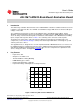
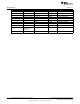
Table 1. Connectors and Test Points
Qty Name Description Application Information
J1 V
IN
Input Voltage Connect to positive terminal of supply voltage.
J2 GND Input Ground Connect to negative terminal of supply voltage (GND).
J3 EN Enable On/Off Jumper connected enables device.
J4 LED+ LED Positive Connect to anode (top) of LED string.
J5 LED- LED Negative Connect to cathode (bottom) of LED string.
J6 BNC Dimming Input Connect a 3V to 10V PWM input signal up to 10 kHz for PWM dimming the LED load.
J7 OUT Output with NTC Alternative connector for LED+ and LED-. Pins 4 and 11 are used for connecting an
external NTC thermistor. Refer to schematic for detailed connectivity.
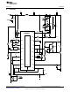
TP1 SW Switch Node Test point for switch node (where Q1, D1, and L1 connect).
Voltage
TP3 SGND Signal Ground Connection for GND when applying signals to TP5, TP8, and TP9.
TP4 LED+ LED Positive Test point for anode (top) of LED string.
Voltage
TP5 nDIM Inverted Dim Signal Test point for dimming input (inverted from input signal).
TP6 V
IN
Input Voltage Test point for input voltage.
TP8 SYNC Synchronization Connect a 3V to 6V PWM clock signal > 500 kHz (pulse width of 100ns) to synchronize
Input the LM3424 switching frequency to the external clock.
TP9 NTC Temp Sense Input Connect a 0V to 1.24V DC voltage to analog dim the LED current.
TP10 PGND Power Ground Test point for GND when monitoring TP1, TP4, or TP6.
2
AN-1967 LM3424 Buck-Boost Evaluation Board SNVA397A–August 2009–Revised May 2013
Submit Documentation Feedback
Copyright © 2009–2013, Texas Instruments Incorporated