
User manual

I
LED
(A)
V
SW
(V)
60
40
20
0
1.0
0.5
0.0
I
LED
2 Ps/DIV
V
SW
I
LED
(A)
V
DIM
(V)
10
5
0
1.0
0.0
-1.0
I
LED
V
DIM
4 ms/DIV
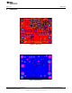
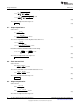
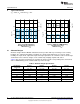
Typical Waveforms
www.ti.com
9 Typical Waveforms
T
A
= +25°C, V
IN
= 24V and V
O
= 21V.
Figure 4. Standard Operation Figure 5. 200Hz 50% PWM Dimming
TP1 Switch Node Voltage (V
SW
) TP5 Dim Voltage (V
DIM
)
LED Current (I
LED
) LED Current (I
LED
)
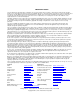
10 Alternate Designs
Alternate designs with the LM3429 evaluation board are possible with very few changes to the existing
hardware. The evaluation board FETs and diodes are already rated higher than necessary for design
flexibility. The input UVLO, output OVP, input and output capacitance can remain the same for the designs
shown below. These alternate designs can be evaluated by changing only R9, R10, and L1.
Table 2 gives the main specifications for four different designs and the corresponding values for R9, R10,
and L1. PWM dimming can be evaluated with any of these designs.
Table 2. Alternate Design Specifications
Specification / Design 1 Design 2 Design 3 Design 4
Component
V
IN
10V - 45V 15V - 50V 20V - 55V 25V - 60V
V
O
14V 21V 28V 35V
f
SW
600kHz 700kHz 500kHz 700kHz
I
LED
2A 500mA 2.5A 1.25A
R9 0.05Ω 0.2Ω 0.04Ω 0.08Ω
R10 12.1 kΩ 10.2 kΩ 14.3 kΩ 10.2 kΩ
L1 22µH 68µH 15µH 33µH
14
AN-1967 LM3424 Buck-Boost Evaluation Board SNVA397A–August 2009–Revised May 2013
Submit Documentation Feedback
Copyright © 2009–2013, Texas Instruments Incorporated