
User manual

www.ti.com
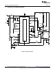
Pin Descriptions
3 Pin Descriptions
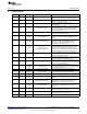
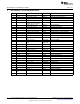
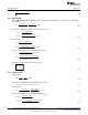
LM3423 LM3421 Name Description Function
Bypass with 100 nF capacitor to AGND as close to
1 1 V
IN
Input Voltage
the device as possible in the circuit board layout.
Connect to AGND for zero current shutdown or
2 2 EN Enable
apply > 2.4V to enable device.
Connect a capacitor to AGND to set the
3 3 COMP Compensation
compensation.
Connect a resistor to AGND to set the signal current.
For analog dimming, connect a controlled current
4 4 CSH Current Sense High
source or a potentiometer to AGND as detailed in
the Analog Dimming section.
External RC network sets the predictive “off-time”
5 5 RCT Resistor Capacitor Timing
and thus the switching frequency.
Connect to PGND through the DAP copper pad to
6 6 AGND Analog Ground provide ground return for CSH, COMP, RCT, and
TIMR.
Connect to a resistor divider from V
O
to program
output over-voltage lockout (OVLO). Turn-off
7 7 OVP Over-Voltage Protection
threshold is 1.24V and hysteresis for turn-on is
provided by 23 µA current source.
Connect a PWM signal for dimming as detailed in
the PWM Dimming section and/or a resistor divider
Dimming Input /
8 8 nDIM from V
IN
to program input under-voltage lockout
Under-Voltage Protection
(UVLO). Turn-on threshold is 1.24V and hysteresis
for turn-off is provided by 23 µA current source.
Connect to pull-up resistor from VIN and N-channel
9 - FLT Fault Flag MosFET open drain output is high when a fault
condition is latched by the timer.
Connect a capacitor to AGND to set the time delay
10 - TIMR Fault Timer
before a sensed fault condition is latched.
Connect to pull-up resistor from VIN and N-channel
11 - LRDY LED Ready Flag MosFET open drain output pulls down when the
LED current is not in regulation.
Connect to AGND if dimming with a series P-
12 - DPOL Dim Polarity channel MosFET or leave open when dimming with
series N-channel MosFET.
13 9 DDRV Dim Gate Drive Output Connect to the gate of the dimming MosFET.
Connect to AGND through the DAP copper pad to
14 10 PGND Power Ground
provide ground return for GATE and DDRV.
15 11 GATE Main Gate Drive Output Connect to the gate of the main switching MosFET.
Bypass with 2.2 µF–3.3 µF ceramic capacitor to
16 12 V
CC
Internal Regulator Output
PGND.
Connect to the drain of the main N-channel MosFET
17 13 IS Main Switch Current Sense switch for R
DS-ON
sensing or to a sense resistor
installed in the source of the same device.
Connect the low side of all external resistor dividers
18 14 RPD Resistor Pull Down (V
IN
UVLO, OVP) to implement “zero-current”
shutdown.
Connect through a series resistor to the positive side
19 15 HSP LED Current Sense Positive
of the LED current sense resistor.
Connect through a series resistor to the negative
20 16 HSN LED Current Sense Negative
side of the LED current sense resistor.
DAP (21) DAP (17) DAP Thermal PAD on bottom of IC Star ground, connecting AGND and PGND.
3
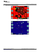
SNVA415C–June 2010–Revised May 2013 AN-2010 LM3423 Buck-Boost 2 Layer Evaluation Board
Submit Documentation Feedback
Copyright © 2010–2013, Texas Instruments Incorporated