
User manual
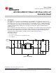

DIMM
1
2
3
6
5
4
VIN
LM3410
C
1
R
1
D
1
LEDs
L
1
R
2
C
2
C
3
R
5
C
4
R
4
D
2
R
3
D
3
J
1
VPWR
C
5
www.ti.com
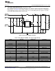
Two Power Supply Design with 12 V > V
PWR
> 5.5 V
6 Two Power Supply Design with 12 V > V
PWR
> 5.5 V
The evaluation board can be modified to allow the user to derive the power from an input supply that is
larger than 5.5 V. In Figure 8, two separate supplies are needed. V
IN
must be between 3.3 V minimum to
5.5 V maximum, but V
VPWR
can be as great as 12 V. The recommended power-up sequence is V
IN
then
V
PWR
. Power-down should be in the reverse order.
Figure 8. Two Power Supply Schematic
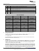
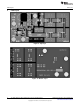
Table 3. Bill of Materials (BOM) - Two Power Supply Design
Part ID Part Value Manufacturer Part Number
U1 2.8A I
SW
LED Driver TI LM3410X
C1, V
IN
, Input Cap 10µF, 6.3 V, X5R TDK C2012X5R0J106M
C2, Output Cap 2.2µF, 25 V, X7R TDK C3225X7R1E225K
C3, Input Cap Placeholder (not stuffed) - -
C4, Output Cap 4.7µF, 25 V, X7R TDK C3225X7R1E475K
C5, V
PWR
, Input Cap 10µF, 25 V, X5R TDK C3225X5R1E106M
D1, Catch Diode 0.4 V
f
Schottky, 500mA ON Semiconductor MBR0530T1G
D2 15 V Zener Diode Central Semiconductor CMHZ4702
D3 0.4 V
f
Schottky, 500mA ON Semiconductor MBR0530T1G
L1 3.3µH, 5.4A Coilcraft DO3316P-332
R1 1Ω, 1% Vishay CRCW12061R00FNEA
R2 Placeholder (not stuffed) - -
R3 100Ω, 1% Vishay CRCW0603100RFKEA
R4 Placeholder (not stuffed) - -
R5 6.8kΩ, 1% Vishay CRCW08056K80FKEA
J1 Jumper Samtec TSW-102-07-T-S
SH-J1 Jumper shunt Tyco Electronics 2-382811-1
LEDs 700mA, V
f
≊ 3 .4 V Cree XPEWHT-L1-0000-008E5
5
SNVA410A–April 2010–Revised May 2013 AN-1996 LM3410X 190mA, LED Driver 6-Pin LLP Evaluation Board
Submit Documentation Feedback
Copyright © 2010–2013, Texas Instruments Incorporated