
User manual

Setting the LED Current
www.ti.com
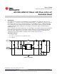
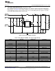
Table 1. Pin Descriptions
Pin Name Function
1 PGND Power ground pin. Place PGND and output capacitor GND close together.
2 V
IN
Supply voltage for power stage, and input supply voltage.
Dimming & shutdown control input. Logic high enables operation. Duty Cycle from 0 to 100%. Do not allow
3 DIM
this pin to float or be greater than V
IN
+ 0.3 V.
4 FB Feedback pin. Connect FB to external resistor divider to set output voltage.
5 AGND Signal ground pin. Place the bottom resistor of the feedback network as close as possible to this pin & pin 4.
6 SW Output switch. Connect to the inductor, output diode.
Signal & Power ground. Connect to pin 1 and pin 5 on top layer. Place 4-6 vias from DAP to bottom layer
DAP GND
GND plane.
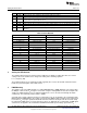
Table 2. Bill of Materials
Part ID Part Value Manufacturer Part Number
U1 2.8A I
SW
LED Driver TI LM3410X
C1, Input Cap 10µF, 6.3 V, X5R TDK C2012X5R0J106M
C2, Output Cap 2.2µF, 25 V, X7R TDK C3225X7R1E225K
C3, Input Cap Placeholder (not stuffed) - -
C4, Output Cap 4.7µF, 25 V, X7R TDK C3225X7R1E475K
D1, Catch Diode 0.4 V
f
Schottky, 500mA ON Semiconductor MBR0530T1G
D2 15 V Zener Diode Central Semiconductor CMHZ4702
D3 0.4 V
f
Schottky, 500mA ON Semiconductor MBR0530T1G
L1 3.3µH, 5.4A Coilcraft DO3316P-332
R1 1Ω, 1% Vishay CRCW12061R00FNEA
R2 Placeholder (not stuffed) - -
R3 100Ω, 1% Vishay CRCW0603100RFKEA
R4 Placeholder (not stuffed) - -
R5 6.8kΩ, 1% Vishay CRCW08056K80FKEA
J1 Jumper Samtec TSW-102-07-T-S
SH-J1 Jumper shunt Tyco Electronics 2-382811-1
LEDs 700mA, V
f
≊ 3.4 V Cree XPEWHT-L1-0000-008E5
2 Setting the LED Current
The default forward current I
LED
delivered to the LED array is 190mA. To adjust this value, the current
setting resistors R1 and R4 can be changed according to the following equation:
I
LED
= (V
FB
)/(R1 || R4)
The feedback voltage V
FB
is regulated at 0.190 V typically. The resistors R1 and R4 should be rated to
handle the power dissipation of the LED current.
3 PWM Dimming
The default set-up of the DIM terminal is to enable PWM dimming. If PWM dimming is not required, then
the DIM pin can be tied to V
IN
through a resistor, R2, using the existing 0805 sized resistor footprint. This
enables the LM3410 whenever V
IN
is applied and allows the set I
LED
current to flow through the LEDs
continuously. A recommended value for R2 is 100kΩ.
A periodic pulse signal at different frequencies and/or duty cycle can be applied to the evaluation board's
DIM terminal for PWM dimming. The voltage measured at the DIM package lead must not be higher than
0.3 V above V
IN
for proper operation. Diode D3 and resistor R5 have been placed in the circuit to clamp
the signal at the DIM lead to no greater than 0.3 V above V
IN
. Although not recommended, a PWM signal
can therefore be applied to the evaluation board DIM terminal with a peak voltage greater than V
IN
.
2
AN-1996 LM3410X 190mA, LED Driver 6-Pin LLP Evaluation Board SNVA410A–April 2010–Revised May 2013
Submit Documentation Feedback
Copyright © 2010–2013, Texas Instruments Incorporated