
User manual
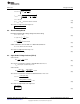

IADJ
EN
CSN
LM3409
UVLO
C1
V
IN
VCC
COFF
GND
CSP
C4
R1
PGATE
C3
R3
R2
DAP
VIN
R4
1
2
3
4
5 6
7
8
9
10
R5
C
5
GND
U1
C2
LED+
LED-
1
2
3
5
6
7
14
13
12
10
9
8
J2
D1
L1
Q1
J1
VADJ
C6
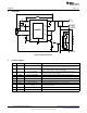
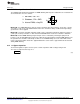
Schematic
www.ti.com
2 Schematic
Figure 2. Board Schematic
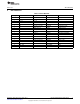
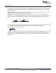
3 Pin Descriptions
Pin(s) Name Description Application Information
1 UVLO Input under-voltage lockout Connect to a resistor divider from V
IN
and GND. Turn-on threshold is
1.24V and hysteresis for turn-off is provided by a 22µA current source.
2 IADJ Analog LED current adjust Apply a voltage between 0 - 1.24V, connect a resistor to GND, or leave
open to set the current sense threshold voltage.
3 EN Logic level enable Apply a voltage >1.74V to enable device, a PWM signal to dim, or a
voltage <0.5V for low power shutdown.
4 COFF Off-time programming Connect resistor to V
O
, and capacitor to GND to set the off-time.
5 GND Ground Connect to the system ground.
6 PGATE Gate drive Connect to the gate of the external PFET.
7 CSN Negative current sense Connect to the negative side of the sense resistor.
8 CSP Positive current sense Connect to the positive side of the sense resistor (V
IN
).
9 VCC V
IN
- referenced linear regulator Connect at least a 1µF ceramic capacitor to V
IN
. The regulator provides
output power for the PFET drive.
10 VIN Input voltage Connect to the input voltage.
DAP DAP Thermal pad on bottom of IC Connect to pin 5 (GND). Place 4-6 vias from DAP to bottom GND plane.
2
AN-1954 LM3409 Demonstration Board SNVA391D–May 2009–Revised May 2013
Submit Documentation Feedback
Copyright © 2009–2013, Texas Instruments Incorporated