
User manual

www.ti.com
Alternate Designs
8 Alternate Designs
Alternate designs with the LM3409 demonstration board are possible with very few changes to the existing
hardware. The evaluation board FETs and diodes are already rated higher than necessary for design
flexibility. The input UVLO can remain the same and the input capacitance is sufficient for most designs,
though the input voltage ripple will change. Other designs can be evaluated by changing R1, R4, L1, and
C5.
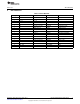
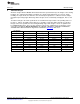
The table below gives the main specifications for four different designs and the corresponding values for
R1, R4, L1, and C5. The RMS current rating of L1 should be at least 50% higher than the specified I
LED
.
Designs 2 and 4 are optimized for best analog dimming range, while designs 1 and 3 are optimized for
best PWM dimming range. These are just examples, however any combination of specifications can be
achieved by following the Design Procedure in the LM3409 / LM3409HV / LM3409Q / LM3409QHV /
LM3409N PFET Buck Controller for High Power LED Drivers (SNVS602) data sheet.
Specification /
Design 1 Design 2 Design 3 Design 4
Component
Dimming Method PWM Analog PWM Analog
V
IN
24V 12V 36V 42V
V
O
14V 7V 24V 35V
f
SW
500 kHz 250 kHz 450 kHz 300 kHz
I
LED
1A 3A 700 mA 2A
Δi
LED
450 mA 70 mA 250 mA 60 mA
R1 15.4 kΩ 15.4 kΩ 25.5 kΩ 24.9 kΩ
R4 0.2Ω 0.08Ω 0.3Ω 0.12Ω
L1 22 µH 33 µH 68 µH 68 µH
C5 None 1 µF None 1 µF
11
SNVA391D–May 2009–Revised May 2013 AN-1954 LM3409 Demonstration Board
Submit Documentation Feedback
Copyright © 2009–2013, Texas Instruments Incorporated