
User manual

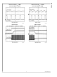

PCB LAYOUT GUIDE
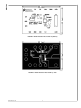
Since copper traces of PCBs carry resistance and parasitic
inductance, the longer the copper trace, the higher the resis-
tance and inductance. These factors introduce voltage and
current spikes to the switching nodes and impair the perfor-
mance of the whole circuit. To optimize the performance of
the LM3407, the rule of thumb is to keep the connections be-
tween components as short and direct as possible. Since true
average current regulation is achieved by detecting the aver-
age switch current, the current setting resistors RISNS1 and
RISNS2 must be located as close to the LM3407 as possible
to reduce the parasitic inductance of the copper trace and
avoid noise pick-up. The connections between LX pin, recti-
fier D1, inductor L1 and output capacitor COUT should be
kept as short as possible to reduce the voltage spikes at the
LX pin. CVCC is the output filter capacitor for the internal lin-
ear regulator of the LM3407, it is recommended to be placed
close to the pin VCC. The input filter capacitor CIN should be
located close to L1 and the cathode of D1. If CIN is connected
to the VIN pin by a long trace, a 0.1µF capacitor should be
added close to pin VIN for noise filtering. In normal operation,
heat will be generated inside the LM3407 and may damage
the device if no thermal management is applied. For more
detail on switching power supply layout considerations see
Application Note AN-1149: Layout Guidelines for Switching
Power Supplies.
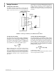
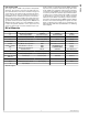
Bill of Materials
Designation Description Package Manufacture Part # Vendor
U1 LED Driver IC, LM3407 eMSOP-8 LM3407 NSC
L1 Inductor 33µH 0.58A 4.0 x 4.0 x 1.8 (mm) LPS4018-333ML Coilcraft
* Inductor 33µH 0.56A 4.8 x 4.3 x 3.5 (mm) CR43NP-330K Sumida
D1 Schottky Diode 40V 1.0A DO-214AC (SMA) SS14 Vishay
CIN, COUT Cap MLCC 50V 4.7µF X7R 1210 GRM32ER71H475K88L Murata
CVCC Cap MLCC 10V 1.0µF X5R 0805 GRM188R61A105KA61D Murata
RISNS1, RISNS2
Chip Resistor 1.13Ω 1%
0805 CRCW08051R13F Vishay
RFS
Chip Resistor 40.2kΩ 1%
0805 CRCW08054022F Vishay
J1 6-pin Connector DIP-12 535676-5 Tyco Electronics
J2 2-way Jumper System 2.54 (mm) Pitch
J3 3-way Jumper System 2.54 (mm) Pitch
VCC, GND, EN, DIM,
ISNS, LX
Terminal pin 2.29 (mm) Dia. 160-1026 Cambion
VIN, GND Terminal pin 1.57 (mm) Dia. 160-1512 Cambion
PCB LM3407 Evaluation Board 59 x 40 (mm) NSC
J3 2-pin Jumper
*Alternative Supplier
7 www.national.com
AN-1763