
User manual


LED DIMMING
There are two ways to disable the current output (I
OUT
) of the
evaluation board circuit. The current output of the LM3407
evaluation board can be disabled by connecting either the
DIM or EN pin to ground. Connecting the EN pin to ground
will shutdown the internal linear regulator and maintain mini-
mal power consumption. Connecting the DIM pin to ground
will only disable the current output of the LM3407, while the
internal oscillator and control circuits remain active to facilitate
fast wake up.
In general, dimming of the LED array can be achieved by ap-
plying a logic pulse chain to the DIM terminal of the evaluation
board to periodically enable and disable the LM3407 and
control the average I
OUT
of the LED array. Since the color
characteristics of a LED are closely related to the driving cur-
rent, dimming by adjusting the current setting resistor causes
the color temperature to drift. To control the brightness of the
LED array effectively, PWM dimming should be used. PWM
dimming is a dimming method which controls the ON/OFF
time ratio of the LED(s) at fixed frequency.
The DIM terminal on the evaluation board is directly connect-
ed to the DIM pin of the LM3407, which provides a PWM
signal input for dimming of the LED array. In order to properly
enable and disable the LM3407, the PWM dimming signal
should have a logic low of 1V maximum and logic high of 2V
minimum. The DIM terminal is internally pulled down to
ground by a 400 kΩ resistor, which should be connected to
either logic high or low and should not be left open. In steady
state, the expression of the average LED driving current is:
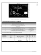
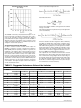
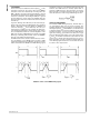
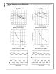
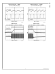
LIMITS OF PWM DIMMING
The maximum PWM dimming frequency, minimum duty cy-
cle, and maximum duty cycle are shown in Figure 6. The
maximum dimming frequency should not exceed 1/50 of the
switching frequency f
SW
of the LM3407. To avoid visible flick-
er, dimming frequencies lower than 100 Hz are not recom-
mended. In Figure 6, T is the period of the PWM dimming
signal. The interval t
D
represents the time delay from a logic
high of the dimming signal and the onset of the output current.
t
SU
and t
SD
are the time needed for the output current to slew
up from zero to steady state and slew down to zero respec-
tively. In the figure, it can be seen that the minimum duty cycle
of the dimming signal should not be shorter than the sum of
t
SU
and t
SD
of the output current.
30046712
FIGURE 6. Limits of the PWM Dimming Signal
www.national.com 6
AN-1763