
Datasheet


www.ti.com
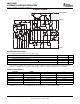
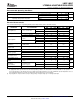
Electrical Characteristics
LM237 , LM337
3-TERMINAL ADJUSTABLE REGULATORS
SLVS047K – NOVEMBER 1981 – REVISED NOVEMBER 2007
T
J
= 25 ° C
LM237, LM337
PARAMETER TEST CONDITIONS
(1)
UNIT
MIN TYP MAX
Input regulation
(2)
V
I
– V
O
= – 3 V to – 40 V 0.01 0.04 %/V
V
O
= – 10 V, f = 120 Hz 60
Ripple rejection dB
V
O
= – 10 V, f = 120 Hz, C
ADJ
= 10 µ F 66 77
|V
O
| ≤ 5 V 50 mV
Output regulation I
O
= 10 mA to 1.5 A
|V
O
| ≥ 5 V 0.3 1 %
Output noise voltage f = 10 Hz to 10 kHz 0.003 %
|V
I
– V
O
| ≤ 40 V 2.5 10
Minimum output current to maintain
mA
regulation
|V
I
– V
O
| ≤ 10 V 1.5 6
|V
I
– V
O
| ≤ 15 V 1.5 2.2
Peak output current A
|V
I
– V
O
| ≤ 40 V 0.15 0.4
ADJUSTMENT current 65 100 µ A
Change in ADJUSTMENT current V
I
– V
O
= – 2.5 V to – 40 V, I
O
= 10 mA to MAX 2 5 µ A
Reference voltage V
I
– V
O
= – 3 V to – 40 V, I
O
= 10 mA to 1.5 A,
– 1.213 – 1.25 – 1.287 V
(OUTPUT to ADJUSTMENT) P ≤ rated dissipation
(1) Unless otherwise noted, the following test conditions apply: |V
I
– V
O
| = 5 V and I
O
= 0.5 A. All characteristics are measured with a
0.1- µ F capacitor across the input and a 1- µ F capacitor across the output. Pulse-testing techniques are used to maintain the junction
temperature as close to the ambient temperature as possible. Thermal effects must be taken into account separately.
(2) Input regulation is expressed here as the percentage change in output voltage per 1-V change at the input.
4 Submit Documentation Feedback Copyright © 1981 – 2007, Texas Instruments Incorporated
Product Folder Link(s): LM237 LM337