
Datasheet
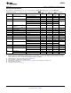

V
C
1
FB
2
SHDN
3
GND
4
SS
8
FSLCT
7
SW
5
V
IN
6
LM3224
SNVS277C –DECEMBER 2004–REVISED MARCH 2013
www.ti.com
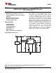
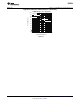
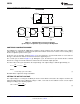
Connection Diagram
Figure 1. 8-Lead Plastic VSSOP
Top View
Package Number DGK0008A
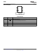
PIN DESCRIPTIONS
Pin Name Function
1 V
C
Compensation network connection. Connected to the output of the voltage error amplifier.
2 FB Output voltage feedback input.
3 SHDN Shutdown control input, active low. This pin has an internal pulldown resistor so the default condition
is off. The pin must be pulled high to turn on the device.
4 GND Analog and power ground.
5 SW Power switch input. Switch connected between SW pin and GND pin.
6 V
IN
Analog power input.
7 FSLCT Switching frequency select input. V
IN
= 1.25MHz. Ground = 615kHz.
8 SS Soft-start Pin.
2 Submit Documentation Feedback Copyright © 2004–2013, Texas Instruments Incorporated
Product Folder Links: LM3224