
Datasheet

:
R
FB2
=
R
FB1
1.26
V
OUT
- 1.26
LM3224
R
FB1
160k
L
10 PH
C
C
1 nF
D1
R
C
30k
C
OUT1
10 PF
R
FB2
30k
SHDN
3
V
IN
6
SW
5
FSLCT
7
GND
4
V
C
1
C1
4.7 PF
D3
C2
4.7 PF
D2
-8V
8V
V
IN
= 2.7V - 5.5V
C
IN
22 PF
C
OUT2
10 PF
D6
C6
1 PF
D5
C4
1 PF
C5
1 PF
D4
D7
C7
1 PF
23V
SS
8
C
SS
C
C2
68 pF
LM3224
SNVS277C –DECEMBER 2004–REVISED MARCH 2013
www.ti.com
APPLICATION INFORMATION
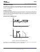
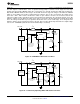
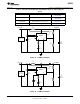
Figure 23. Triple Output TFT Bias (615 kHz operation)
TRIPLE OUTPUT TFT BIAS
The circuit in Figure 23 shows how the LM3224 can be configured to provide outputs of 8V, −8V, and 23V,
convenient for biasing TFT displays. The 8V output is regulated, while the −8V and 23V outputs are unregulated.
The 8V output is generated by a typical boost topology. The basic operation of the boost converter is described
in the OPERATION section. The output voltage is set with R
FB1
and R
FB2
by:
(22)
The compensation network of R
C
and C
C
are chosen to optimally stabilize the converter. The inductor also
affects the stability. When operating at 615 kHz, a 10uH inductor is recommended to insure the converter is
stable at duty cycles greater than 50%. Refer to the COMPENSATION section for more information.
The -8V output is derived from a diode inverter. During the second cycle, when the transistor is open, D2
conducts and C1 charges to 8V minus a diode drop (≊0.4V if using a Schottky). When the transistor opens in the
first cycle, D3 conducts and C1's polarity is reversed with respect to the output at C2, producing -8V.
16 Submit Documentation Feedback Copyright © 2004–2013, Texas Instruments Incorporated
Product Folder Links: LM3224