
Datasheet

f
PC2
=
1
2SC
C2
(R
C
//R
O
)
(in Hz)
f
ZC
=
1
2SC
C
R
C
(in Hz)
LM3224
www.ti.com
SNVS277C –DECEMBER 2004–REVISED MARCH 2013
Since R
C
is generally much less than R
O
, it does not have much effect on the above equation and can be
neglected until a value is chosen to set the zero f
ZC
. f
ZC
is created to cancel out the pole created by the output
capacitor, f
P1
. The output capacitor pole will shift with different load currents as shown by the equation, so setting
the zero is not exact. Determine the range of f
P1
over the expected loads and then set the zero f
ZC
to a point
approximately in the middle. The frequency of this zero is determined by:
(19)
Now R
C
can be chosen with the selected value for C
C
. Check to make sure that the pole f
PC
is still in the 10Hz to
500Hz range, change each value slightly if needed to ensure both component values are in the recommended
range.
HIGH OUTPUT CAPACITOR ESR COMPENSATION
When using an output capacitor with a high ESR value, or just to improve the overall phase margin of the control
loop, another pole may be introduced to cancel the zero created by the ESR. This is accomplished by adding
another capacitor, C
C2
, directly from the compensation pin V
C
to ground, in parallel with the series combination of
R
C
and C
C
. The pole should be placed at the same frequency as f
Z1
, the ESR zero. The equation for this pole
follows:
(20)
To ensure this equation is valid, and that C
C2
can be used without negatively impacting the effects of R
C
and C
C
,
f
PC2
must be greater than 10f
ZC
.
CHECKING THE DESIGN
With all the poles and zeros calculated the crossover frequency can be checked as described in the section DC
Gain and Open-loop Gain. The compensation values can be changed a little more to optimize performance if
desired. This is best done in the lab on a bench, checking the load step response with different values until the
ringing and overshoot on the output voltage at the edge of the load steps is minimal. This should produce a
stable, high performance circuit. For improved transient response, higher values of R
C
should be chosen. This
will improve the overall bandwidth which makes the regulator respond more quickly to transients. If more detail is
required, or the most optimum performance is desired, refer to a more in depth discussion of compensating
current mode DC/DC switching regulators.
POWER DISSIPATION
The output power of the LM3224 is limited by its maximum power dissipation. The maximum power dissipation is
determined by the formula
P
D
= (T
jmax
- T
A
)/θ
JA
where
• T
jmax
is the maximum specidfied junction temperature (125°C)
• T
A
is the ambient temperature
• θ
JA
is the thermal resistance of the package (21)
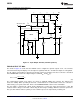
LAYOUT CONSIDERATIONS
The input bypass capacitor C
IN
, as shown in the typical operating circuit, must be placed close to the IC. This will
reduce copper trace resistance which effects input voltage ripple of the IC. For additional input voltage filtering, a
100nF bypass capacitor can be placed in parallel with C
IN
, close to the V
IN
pin, to shunt any high frequency noise
to ground. The output capacitor, C
OUT
, should also be placed close to the IC. Any copper trace connections for
the C
OUT
capacitor can increase the series resistance, which directly effects output voltage ripple. The feedback
network, resistors R
FB1
and R
FB2
, should be kept close to the FB pin, and away from the inductor, to minimize
copper trace connections that can inject noise into the system. Trace connections made to the inductor and
schottky diode should be minimized to reduce power dissipation and increase overall efficiency. For more detail
on switching power supply layout considerations see Application Note Layout Guidelines for Switching Power
Supplies (SNVA021).
Copyright © 2004–2013, Texas Instruments Incorporated Submit Documentation Feedback 15
Product Folder Links: LM3224