
Datasheet

'i
L
=
(in Amps)
V
IN
D
2Lfs
V
IN
R
DSON
0.144 fs
L >
(in H)
)(
D
D'
-1
Hz
1
2S(R
C
+ R
O
)C
C
f
PC
=
Hz
1
f
ZC
=
2SR
C
C
C
LM3224
SNVS277C –DECEMBER 2004–REVISED MARCH 2013
www.ti.com
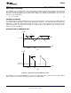
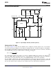
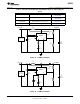
To keep a current programmed control converter stable above duty cycles of 50%, the inductor must meet
certain criteria. The inductor, along with input and output voltage, will determine the slope of the current through
the inductor (see Figure 22 (a)). If the slope of the inductor current is too great, the circuit will be unstable above
duty cycles of 50%. A 10µH to 15µH inductor is recommended for most 615 kHz applications, while a 4.7µH to
10µH inductor may be used for most 1.25 MHz applications. If the duty cycle is approaching the maximum of
85%, it may be necessary to increase the inductance by as much as 2X. See Inductor and Diode Selection for
more detailed inductor sizing.
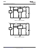
The LM3224 provides a compensation pin (V
C
) to customize the voltage loop feedback. It is recommended that a
series combination of R
C
and C
C
be used for the compensation network, as shown in the typical application
circuit. For any given application, there exists a unique combination of R
C
and C
C
that will optimize the
performance of the LM3224 circuit in terms of its transient response. The series combination of R
C
and C
C
introduces a pole-zero pair according to the following equations:
(4)
where
• R
O
is the output impedance of the error amplifier (approximately 900kΩ) (5)
For most applications, performance can be optimized by choosing values within the range 5kΩ ≤ R
C
≤ 100kΩ (R
C
can be up to 200kΩ if C
C2
is used, see High Output Capacitor ESR Compensation) and 680pF ≤ C
C
≤ 10nF.
Refer to the Applications Information section for recommended values for specific circuits and conditions. Refer
to the Compensation section for other design requirement.
COMPENSATION
This section will present a general design procedure to help insure a stable and operational circuit. The designs
in this datasheet are optimized for particular requirements. If different conversions are required, some of the
components may need to be changed to ensure stability. Below is a set of general guidelines in designing a
stable circuit for continuous conduction operation, in most all cases this will provide for stability during
discontinuous operation as well. The power components and their effects will be determined first, then the
compensation components will be chosen to produce stability.
INDUCTOR AND DIODE SELECTION
Although the inductor sizes mentioned earlier are fine for most applications, a more exact value can be
calculated. To ensure stability at duty cycles above 50%, the inductor must have some minimum value
determined by the minimum input voltage and the maximum output voltage. This equation is:
where
• fs is the switching frequency
• D is the duty cycl
• R
DSON
is the ON resistance of the internal switch taken from the graph "NMOS R
DSON
vs. Input Voltage" in the
Typical Performance Characteristics section. (6)
This equation is only good for duty cycles greater than 50% (D>0.5), for duty cycles less than 50% the
recommended values may be used. The corresponding inductor current ripple as shown in Figure 22 (a) is given
by:
(7)
12 Submit Documentation Feedback Copyright © 2004–2013, Texas Instruments Incorporated
Product Folder Links: LM3224