
Datasheet

:
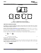
R
FB1
= R
FB2
x
V
OUT
- 1.26
1.26
V
OUT
=
V
IN
1-D
, D' = (1-D) =
V
IN
V
OUT
V
IN
C
OUT
PWM
L
R
LOAD
V
IN
L
C
OUT
R
LOAD
X
V
IN
L
C
OUT
R
LOAD
Cycle 1 Cycle 2
(a)
(b)
+
V
OUT
-
+
V
OUT
-
D
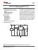
LM3224
SNVS277C –DECEMBER 2004–REVISED MARCH 2013
www.ti.com
OPERATION
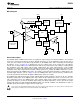
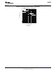
Figure 21. Simplified Boost Converter Diagram
(a) First Cycle of Operation (b) Second Cycle Of Operation
CONTINUOUS CONDUCTION MODE
The LM3224 is a current-mode, PWM boost regulator. A boost regulator steps the input voltage up to a higher
output voltage. In continuous conduction mode (when the inductor current never reaches zero at steady state),
the boost regulator operates in two cycles.
In the first cycle of operation, shown in Figure 21 (a), the transistor is closed and the diode is reverse biased.
Energy is collected in the inductor and the load current is supplied by C
OUT
.
The second cycle is shown in Figure 21 (b). During this cycle, the transistor is open and the diode is forward
biased. The energy stored in the inductor is transferred to the load and output capacitor.
The ratio of these two cycles determines the output voltage. The output voltage is defined approximately as:
where
• D is the duty cycle of the switch (1)
D and D′ will be required for design calculations.
SETTING THE OUTPUT VOLTAGE
The output voltage is set using the feedback pin and a resistor divider connected to the output as shown in the
typical operating circuit. The feedback pin voltage is 1.26V, so the ratio of the feedback resistors sets the output
voltage according to the following equation:
(2)
10 Submit Documentation Feedback Copyright © 2004–2013, Texas Instruments Incorporated
Product Folder Links: LM3224