
Datasheet


LM3151, LM3152, LM3153
SNVS562G –SEPTEMBER 2008–REVISED MARCH 2011
www.ti.com
These devices have limited built-in ESD protection. The leads should be shorted together or the device placed in conductive foam
during storage or handling to prevent electrostatic damage to the MOS gates.
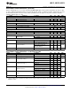
ABSOLUTE MAXIMUM RATINGS
(1)(2)
VIN to GND -0.3V to 47V
SW to GND -3V to 47V
BST to SW -0.3V to 7V
BST to GND -0.3V to 52V
All Other Inputs to GND -0.3V to 7V
ESD Rating
(3)
2kV
Storage Temperature Range -65°C to +150°C
(1) Absolute Maximum Ratings indicate limits beyond which damage to the device may occur. Operating Ratings indicate conditions for
which the device is intended to be functional, but does not ensure specific performance limits. For ensured specifications and conditions,
see the Electrical Characteristics.
(2) If Military/Aerospace specified devices are required, please contact the Texas Instruments Sales Office/Distributors for availability and
specifications.
(3) The human body model is a 100 pF capacitor discharged through a 1.5 kΩ resistor into each pin. Test Method is per JESD-22-A114.
OPERATING RATINGS
(1)
V
IN
6V to 42V
Junction Temperature Range (T
J
) −40°C to + 125°C
EN 0V to 5V
(1) Absolute Maximum Ratings indicate limits beyond which damage to the device may occur. Operating Ratings indicate conditions for
which the device is intended to be functional, but does not ensure specific performance limits. For ensured specifications and conditions,
see the Electrical Characteristics.
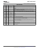
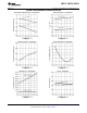
ELECTRICAL CHARACTERISTICS
Limits in standard type are for T
J
= 25°C only; limits in boldface type apply over the junction temperature (T
J
) range of -40°C
to +125°C. Minimum and Maximum limits are specified through test, design, or statistical correlation. Typical values represent
the most likely parametric norm at T
J
= 25°C, and are provided for reference purposes only. Unless otherwise stated the
following conditions apply: V
IN
= 18V.
Symbol Parameter Conditions Min Typ Max Units
Start-Up Regulator, VCC
V
CC
C
VCC
= 1 µF, 0 mA to 40 mA 5.65 5.95 6.25 V
I
VCC
= 2 mA, Vin = 5.5V 40
V
IN
- V
CC
V
IN
- V
CC
Dropout Voltage mV
I
VCC
= 30 mA, Vin = 5.5V 330
I
VCCL
V
CC
Current Limit
(1)
V
CC
= 0V 65 100 mA
VCC Under-voltage Lockout threshold 4.75 5.1 5.40
VCC
UVLO
VCC Increasing V
(UVLO)
V
CC-UVLO-HYS
V
CC
UVLO Hysteresis VCC Decreasing 475 mV
t
CC-UVLO-D
V
CC
UVLO Filter Delay 3 µs
I
IN
Input Operating Current No Switching 3.6 5.2 mA
I
IN-SD
Input Operating Current, Device Shutdown V
EN
= 0V 32 55 µA
GATE Drive
I
Q-BST
Boost Pin Leakage V
BST
– V
SW
= 6V 2 nA
R
DS-HG-Pull-Up
HG Drive Pull–Up On-Resistance I
HG
Source = 200 mA 5 Ω
R
DS-HG-Pull-Down
HG Drive Pull–Down On-Resistance I
HG
Sink = 200 mA 3.4 Ω
R
DS-LG-Pull-Up
LG Drive Pull–Up On-Resistance I
LG
Source = 200 mA 3.4 Ω
R
DS-LG-Pull-Down
LG Drive Pull–Down On-Resistance I
LG
Sink = 200 mA 2 Ω
(1) VCC provides self bias for the internal gate drive and control circuits. Device thermal limitations limit external loading.
4 Submit Documentation Feedback Copyright © 2008–2011, Texas Instruments Incorporated
Product Folder Links: LM3151 LM3152 LM3153