
Datasheet


LM3151, LM3152, LM3153
www.ti.com
SNVS562G –SEPTEMBER 2008–REVISED MARCH 2011
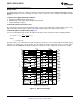
Bill of Materials
Designator Value Parameters Manufacturer Part Number
C
BST
0.47 µF Ceramic, X7R, 16V, 10% TDK C2012X7R1C474K
C
BYP
0.1 µF Ceramic, X7R, 50V, 10% TDK C2012X7R1H104K
C
EN
1000 pF Ceramic, X7R, 50V, 10% TDK C1608X7R1H102K
C
IN1
100 µF AL, EEV-FK, 63V, 20% Panasonic EEV-FK1J101P
C
IN2
, C
IN3
10 µF Ceramic, X5R, 35V, 10% Taiyo Yuden GMK325BJ106KN-T
C
OUT1
, C
OUT2
150 µF AL, UE, 6.3V, 20% Panasonic EEF-UE0J151R
C
SS
0.068 µF Ceramic, 16V, 10% 0603YC683KAT2A
C
VCC
1 µF Ceramic, X7R, 16V, 10% Kemet C0805C105K4RACTU
L1 1.65 µH Shielded Drum Core, A, 2.53 mΩ Coilcraft Inc. HA3778-AL
M1, M2 30V 8 nC, R
DS(ON)
@4.5V = 10 mΩ Renesas RJK0305DB
U1 Texas Instruments LM3152MH-3.3
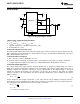
PCB Layout Considerations
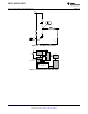
It is good practice to layout the power components first, such as the input and output capacitors, FETs, and
inductor. The first priority is to make the loop between the input capacitors and the source of the low side FET to
be very small and tie the grounds of each directly to each other and then to the ground plane through vias. As
shown in the figure below, when the input cap ground is tied directly to the source of the low side FET, parasitic
inductance in the power path, along with noise coupled into the ground plane, are reduced.
The switch node is the next item of importance. The switch node should be made only as large as required to
handle the load current. There are fast voltage transitions occurring in the switch node at a high frequency, and if
the switch node is made too large it may act as an antennae and couple switching noise into other parts of the
circuit. For high power designs it is recommended to use a multi-layer board. The FET’s are going to be the
largest heat generating devices in the design, and as such, care should be taken to remove the heat. On multi
layer boards using exposed-pad packages for the FET’s such as the power-pak SO-8, vias should be used under
the FETs to the same plane on the interior layers to help dissipate the heat and cool the FETs. For the typical
single FET Power-Pak type FETs the high-side FET DAP is Vin. The Vin plane should be copied to the other
interior layers to the bottom layer for maximum heat dissipation. Likewise, the DAP of the low-side FET is
connected to the SW node and it’s shape should be duplicated to the interior layers down to the bottom layer for
maximum heat dissipation.
See the Evaluation Board application note AN-1900 (literature number (SNVA371) for an example of a typical
multilayer board layout, and the Demonstration Board Reference Design App Note for a typical 2 layer board
layout. Each design allows for single sided component mounting.
Copyright © 2008–2011, Texas Instruments Incorporated Submit Documentation Feedback 19
Product Folder Links: LM3151 LM3152 LM3153