
Datasheet


Table Of Contents
LM3150
SNVS561D –SEPTEMBER 2008–REVISED MARCH 2011
www.ti.com
Electrical Characteristics (continued)
Limits in standard type are for T
J
= 25°C only; limits in boldface type apply over the junction temperature (T
J
) range of -40°C
to +125°C. Minimum and Maximum limits are specified through test, design, or statistical correlation. Typical values represent
the most likely parametric norm at T
J
= 25°C, and are provided for reference purposes only. Unless otherwise stated the
following conditions apply: V
IN
= 18V.
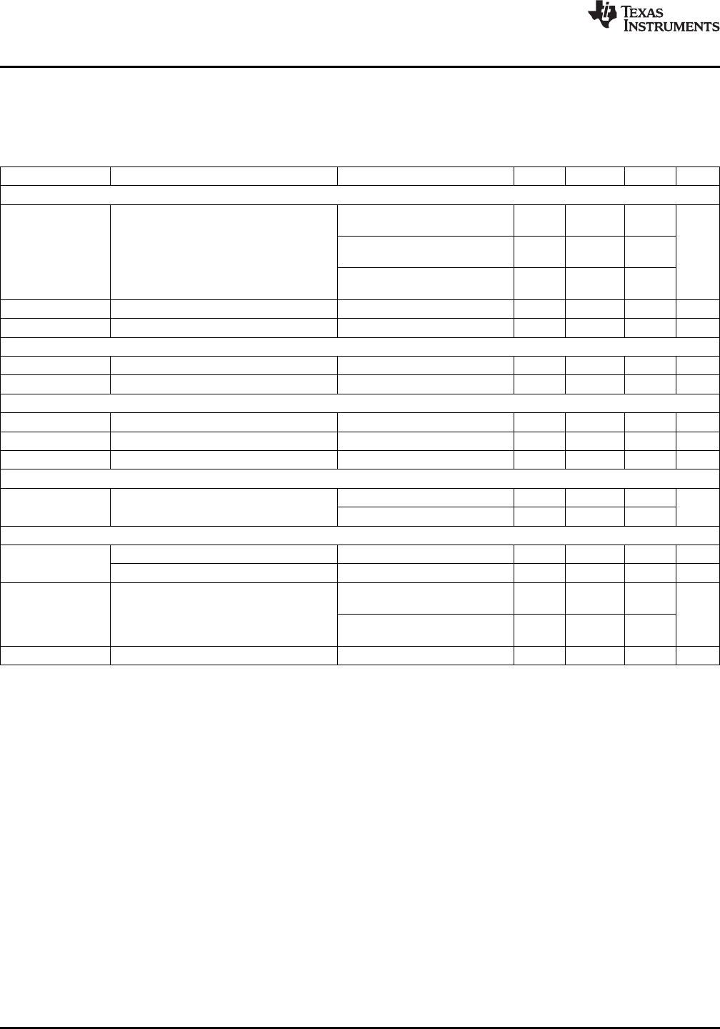
Symbol Parameter Conditions Min Typ Max Units
ON/OFF Timer
V
IN
= 10V, R
ON
= 100 kΩ,
1.02
V
FB
= 0.6V
V
IN
= 18V, R
ON
= 100 kΩ,
t
ON
ON Timer Pulse Width 0.62 µs
V
FB
= 0.6V
V
IN
= 42V, R
ON
= 100 kΩ,
0.36
V
FB
= 0.6V
t
ON-MIN
ON Timer Minimum Pulse Width See
(2)
200 ns
t
OFF
OFF Timer Minimum Pulse Width 370 525 ns
Enable Input
V
EN
EN Pin Input Threshold Trip Point V
EN
Rising 1.14 1.20 1.26 V
V
EN-HYS
EN Pin Threshold Hysteresis V
EN
Falling 120 mV
Regulation and Over-Voltage Comparator
V
FB
In-Regulation Feedback Voltage V
SS
> 0.6V 0.588 0.600 0.612 V
V
FB-OV
Feedback Over-Voltage Threshold 0.690 0.720 0.748 V
I
FB
Feedback Bias Current 20 nA
Boost Diode
Forward Voltage I
BST
= 2 mA 0.7
V
f
V
I
BST
= 30 mA 1
Thermal Characteristics
Thermal Shutdown Rising 165 °C
T
SD
Thermal Shutdown Hysteresis Falling 15 °C
4 Layer JEDEC Printed Circuit
40
Board, 9 Vias, No Air Flow
θ
JA
Junction to Ambient °C/W
2 Layer JEDEC Printed Circuit
140
Board. No Air Flow
θ
JC
Junction to Case No Air Flow 4 °C/W
(2) See Theory of Operation section for minimum on-time when using MOSFETs connected to gate drivers.
4 Submit Documentation Feedback Copyright © 2008–2011, Texas Instruments Incorporated
Product Folder Links: LM3150