
Datasheet


Table Of Contents
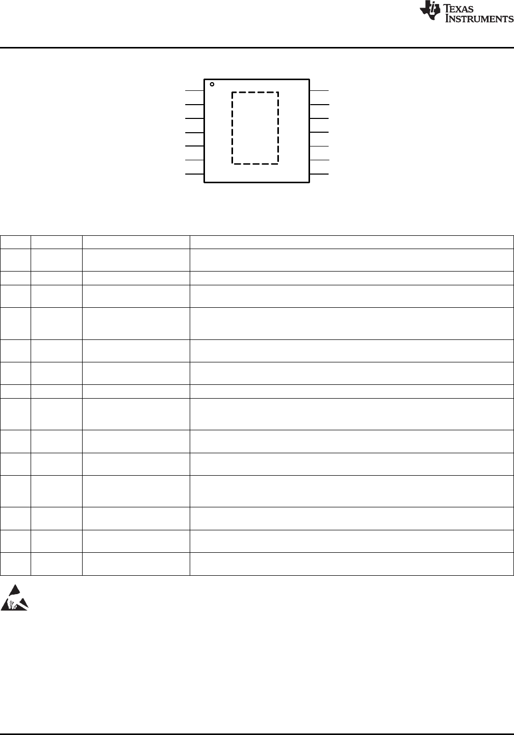
1
2
3
4
11
12
13
14
HG
VCC
5
6
7
SGND
PGND
8
9
SS
RON
LG
EN
10
SW
FB
SGND
ILIM
BST
VIN
EP
LM3150
SNVS561D –SEPTEMBER 2008–REVISED MARCH 2011
www.ti.com
Connection Diagram
Figure 1. TSSOP-14
PIN DESCRIPTIONS
Pin Name Description Function
Supply Voltage for FET Nominally regulated to 5.95V. Connect a 1.0 µF to 4.7 µF decoupling capacitor from
1 VCC
Drivers this pin to ground.
2 VIN Input Supply Voltage Supply pin to the device. Nominal input range is 6V to 42V.
To enable the IC apply a logic high signal to this pin greater than 1.26V typical or leave
3 EN Enable
floating. To disable the part, ground the EN pin.
Internally connected to the regulation, over-voltage, and short-circuit comparators. The
4 FB Feedback regulation setting is 0.6V at this pin. Connect to feedback resistor divider between the
output and ground to set the output voltage.
Ground for all internal bias and reference circuitry. Should be connected to PGND at a
5,9 SGND Signal Ground
single point.
An internal 7.7 µA current source charges an external capacitor to provide the soft-start
6 SS Soft-Start
function.
7 RON On-time Control An external resistor from VIN to this pin sets the high-side switch on-time.
Monitors current through the low-side switch and triggers current limit operation if the
8 ILIM Current Limit inductor valley current exceeds a user defined value that is set by R
LIM
and the Sense
current, I
LIM-TH
, sourced out of this pin during operation.
Switch pin of controller and high-gate driver lower supply rail. A boost capacitor is also
10 SW Switch Node
connected between this pin and BST pin
Gate drive signal to the high-side NMOS switch. The high-side gate driver voltage is
11 HG High-Side Gate Drive
supplied by the differential voltage between the BST pin and SW pin.
High-gate driver upper supply rail. Connect a 0.33 µF-0.47 µF capacitor from SW pin to
Connection for Bootstrap
12 BST this pin. An internal diode charges the capacitor during the high-side switch off-time. Do
Capacitor
not connect to an external supply rail.
Gate drive signal to the low-side NMOS switch. The low-side gate driver voltage is
13 LG Low-Side Gate Drive
supplied by VCC.
Synchronous rectifier MOSFET source connection. Tie to power ground plane. Should
14 PGND Power Ground
be tied to SGND at a single point.
Exposed die attach pad should be connected directly to SGND. Also used to help
EP EP Exposed Pad
dissipate heat out of the IC.
These devices have limited built-in ESD protection. The leads should be shorted together or the device placed in conductive foam
during storage or handling to prevent electrostatic damage to the MOS gates.
2 Submit Documentation Feedback Copyright © 2008–2011, Texas Instruments Incorporated
Product Folder Links: LM3150