
Datasheet


Table Of Contents
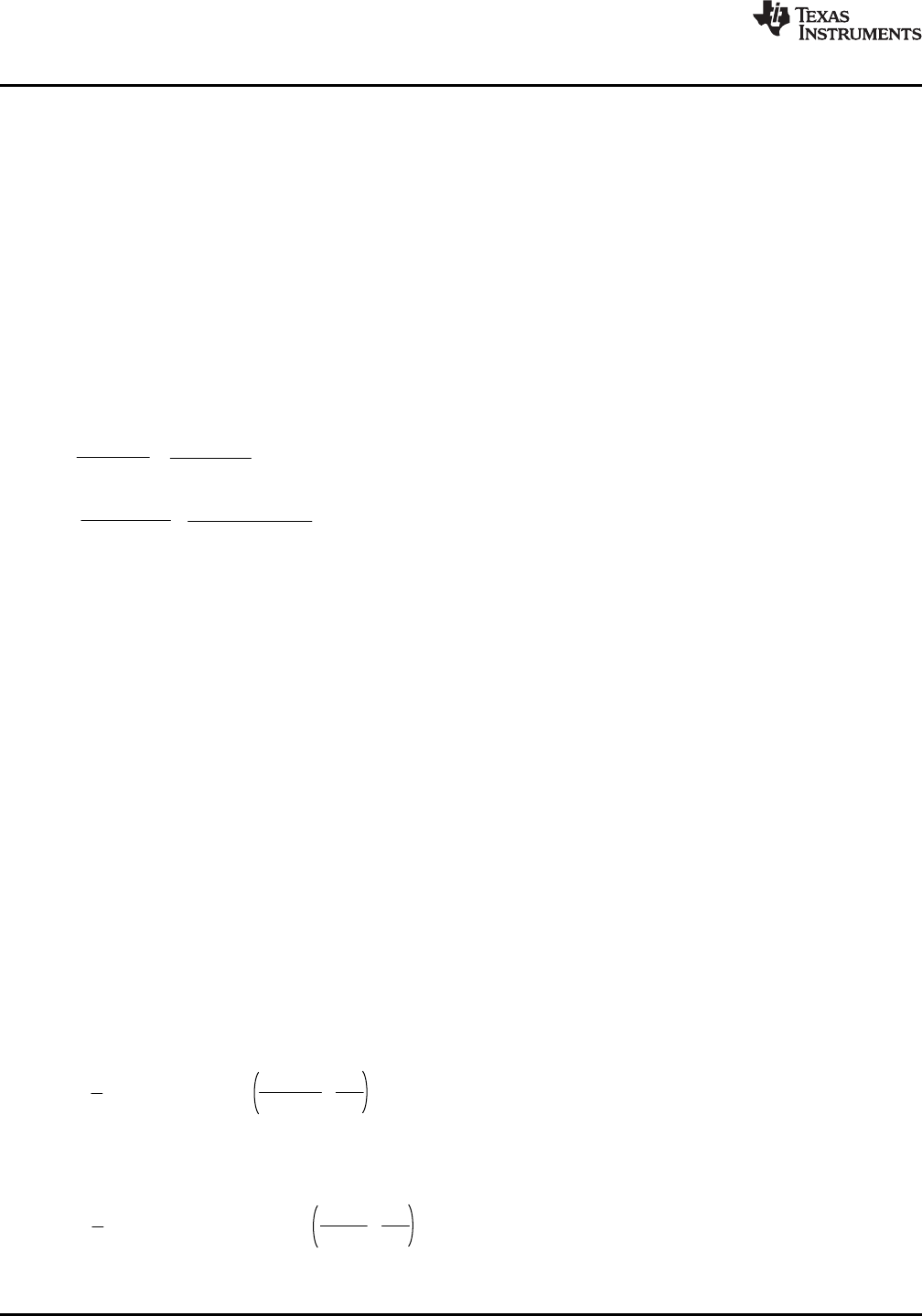
Pdh = 0.396 + 0.278 = 0.674W
Pcond = I
out
2
x
R
DS(ON)
x D
8.5
Vcc - Vth
+
6.8
Vth
1
2
x V
in
x I
out
x Q
gd
x f
s
x
Psw =
Pdh = Pcond + Psw
Pcond = 12
2
x 0.01 x 0.275 = 0.396W
8.5
6 ± 2.5
+
6.8
2.5
1
2
x 12 x 12 x 1.5 nC x 500 kHz x
Psw =
= 0.278W
C
ff
=
V
IN-MIN
x f
s
V
OUT
x
R
FB1
+ R
FB2
R
FB1
x R
FB2
C
ff
=
6V x 500 kHz
3.3V
x
4.99 k: + 22.6 k:
4.99 k: x 22.6 k:
= 269 pF
LM3150
SNVS561D –SEPTEMBER 2008–REVISED MARCH 2011
www.ti.com
For this design a feed-forward capacitor will be used to help minimize output ripple.
ESR
max
= (80 mV x 1.65 µH x 1) / 5.7 V µs
ESR
max
= 23 mΩ
The minimum ESR must meet both of the following criteria:
ESR
min
≥ (15 mV x L x A
f
) / ET
ESR
min
≥ [ ET / (V
IN
- V
OUT
) ] x (A
f
/ C
O
)
ESR
min
≥ (15 mV x 1.65 µH x 1) / 5.7 V µs = 4.3 mΩ
ESR
min
≥ [5.7 V µs / (12 - 3.3) ] x (1 / 169 µF) = 3.9 mΩ
Based on the above criteria two 150 µF polymer aluminum capacitors with a ESR = 12 mΩ each for a effective
ESR in parallel of 6 mΩ was chosen from Panasonic. The part number is EEF-UE0J101P.
6. Determine Use of Feed-Forward Capacitor
From step 5 the capacitor chosen in ESR is small enough that we should use a feed-forward capacitor. This is
calculated from:
Let C
ff
= 270 pF, which is the closest next standard value.
7. MOSFET and R
LIM
Selection
The LM3150 is designed to drive N-channel MOSFETs. For a maximum input voltage of 24V we should choose
N-channel MOSFETs with a maximum drain-source voltage, V
DS
, greater than 1.2 x 24V = 28.8V. FETs with
maximum V
DS
of 30V will be the first option. The combined total gate charge Q
gtotal
of the high-side and low-side
FET should satisfy the following:
Q
gtotal
≤ I
VCCL
/ f
s
Q
gtotal
≤ 65 mA / 500 kHz
Q
gtotal
≤ 130 nC
Where I
VCCL
is the minimum current limit of VCC, over the temperature range, specified in the Electrical
Characteristics table. The MOSFET gate charge Q
g
is gathered from reading the V
GS
vs Q
g
curve of the
MOSFET datasheet at the V
GS
= 5V for the high-side, M1, MOSFET and V
GS
= 6V for the low-side, M2,
MOSFET.
The Renesas MOSFET RJK0305DPB has a gate charge of 10 nC at V
GS
= 5V, and 12 nC at V
GS
= 6V. This
combined gate charge for a high-side, M1, and low-side, M2, MOSFET 12 nC + 10 nC = 22 nC is less than 130
nC calculated Q
gtotal
.
The calculated MOSFET power dissipation must be less than the max allowed power dissipation, Pdmax, as
specified in the MOSFET datasheet. An approximate calculation of the FET power dissipated Pd, of the high-side
and low-side FET is given by:
High-Side MOSFET
18 Submit Documentation Feedback Copyright © 2008–2011, Texas Instruments Incorporated
Product Folder Links: LM3150