
Datasheet


Table Of Contents
R
FB2
= 4.99 k:
3.3V
0.6V
-1
R
FB2
= R
FB1
V
OUT
V
FB
-1
EN
SS
HG
SW
L
LM3150
FB
VCC
PGND
SGND
BST
ILIM
LG
C
BYP
C
SS
V
IN
VIN
R
ON
RON
C
OUT
V
OUT
C
BST
C
VCC
V
IN
R
LIM
R
FB2
R
FB1
M2
M1
C
EN
C
FF
C
IN
C
SS
=
I
SS
x t
SS
V
ref
LM3150
SNVS561D –SEPTEMBER 2008–REVISED MARCH 2011
www.ti.com
9. Calculate Soft-Start Capacitor
where
• t
ss
is the soft-start time in seconds
• V
ref
= 0.6V (27)
10. C
VCC
, C
BST
and C
EN
C
VCC
should be placed directly at the VCC pin with a recommended value of 1 µF to 4.7 µF. C
BST
creates a
voltage used to drive the gate of the high-side FET. It is charged during the SW off-time. The recommended
value for C
BST
is 0.47 µF. The EN bypass capacitor, C
EN
, recommended value is 1000 pF when driving the EN
pin from open drain type of signal.
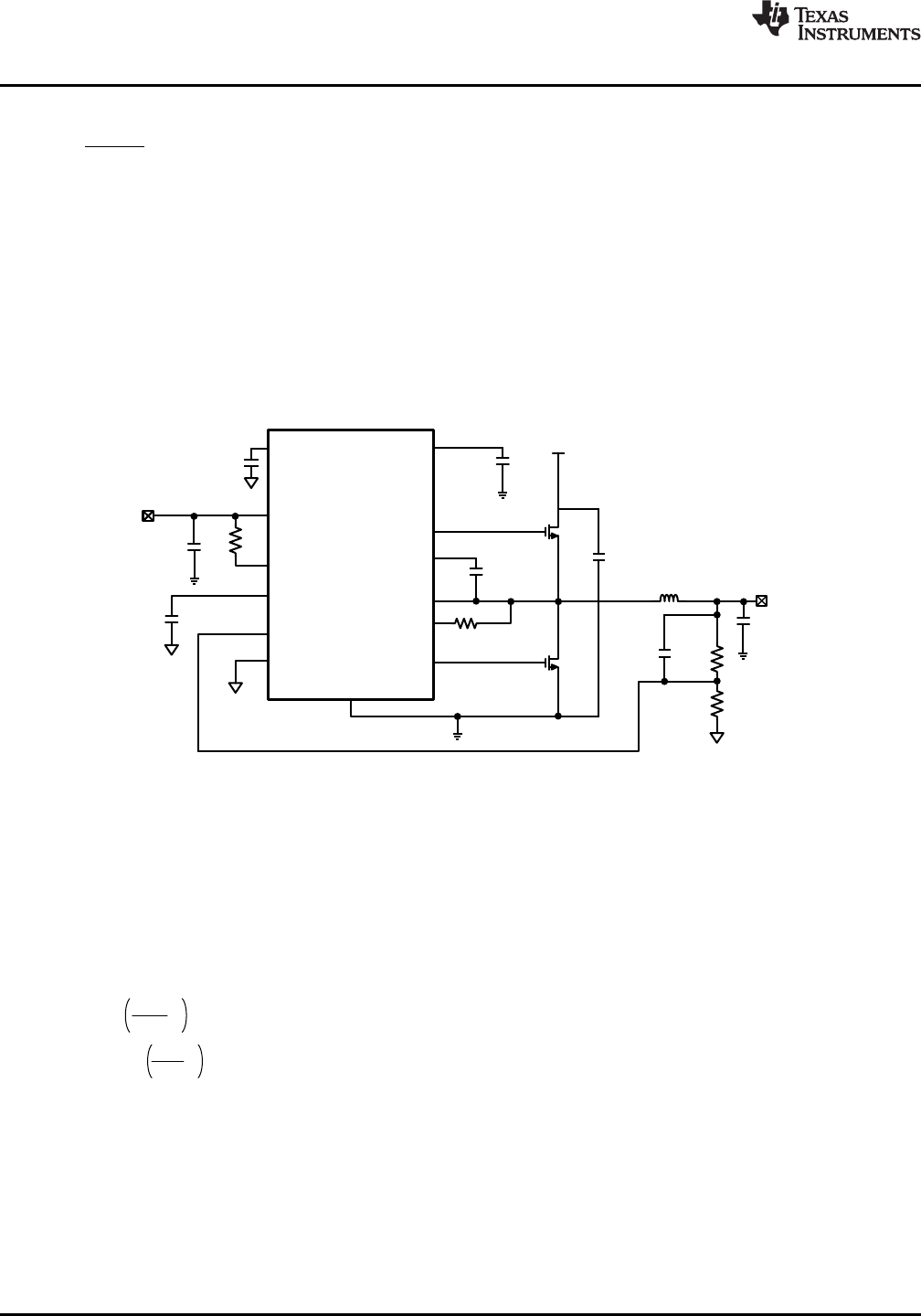
Design Example
Figure 16. Design Example Schematic
1.Define Power Supply Operating Conditions
a. V
OUT
= 3.3V
b. V
IN-MIN
= 6V, V
IN-TYP
= 12V, V
IN-MAX
= 24V
c. Typical Load Current = 12A, Max Load Current = 15A
d. Soft-Start time t
SS
= 5 ms
2. Set Output Voltage with Feedback Resistors
R
FB2
= 22.455 kΩ
R
FB2
= 22.6 kΩ, nearest 1% standard value.
3. Determine R
ON
and f
S
D
min
= V
OUT
/V
IN-MAX
D
min
= 3.3V/24V = 0.137
D
max
= 3.3V / 6V = 0.55
f
smax
= 0.137/ 200 ns = 687 kHz
D
max
= V
OUT
/V
IN-MIN
16 Submit Documentation Feedback Copyright © 2008–2011, Texas Instruments Incorporated
Product Folder Links: LM3150