
Datasheet


Table Of Contents
C
IN
=
Iomax x D x (1-D)
f
s
x 'V
IN-MAX
R
LIM
(T
j
) =
I
CL
x R
DS(ON)max
I
LIM-TH
(T
j
)
LM3150
www.ti.com
SNVS561D –SEPTEMBER 2008–REVISED MARCH 2011
Z
FB
= (R
FB1
x R
FB2
)/(R
FB1
+ R
FB2
) (21)
C
ff
= V
OUT
/(V
IN-MIN
x f
S
x Z
FB
) (22)
7. MOSFET and R
LIM
Selection
The high-side and low-side FETs must have a drain to source (V
DS
) rating of at least 1.2 x V
IN
.
Use the following equations to calculate the desired target value of the low-side FET R
DS(ON)
for current limit.
(23)
I
LIM-TH
(T
j
) = I
LIM-TH
x [1 + 3.3 x 10
-3
x (T
j
- 27)] (24)
The gate drive current from VCC must not exceed the minimum current limit of VCC. The drive current from VCC
can be calculated with:
I
VCCdrive
= Q
gtotal
x f
S
where
• Q
gtotal
is the combined total gate charge of the high-side and low-side FETs (25)
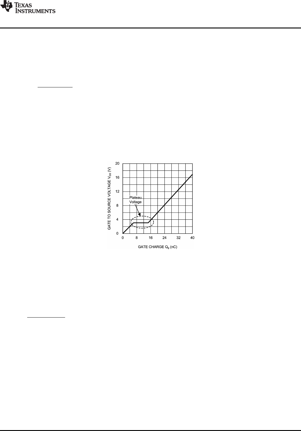
The plateau voltage of the FET V
GS
vs Q
g
curve, as shown in Figure 15, must be less than VCC - 750 mV.
Figure 15. Typical MOSFET Gate Charge Curve
See following design example for estimated power dissipation calculation.
8. Calculate Input Capacitance
The main parameters for the input capacitor are the voltage rating, which must be greater than or equal to the
maximum DC input voltage of the power supply, and its rms current rating. The maximum rms current is
approximately 50% of the maximum load current.
where
• ΔV
IN-MAX
is the maximum allowable input ripple voltage (26)
A good starting point for the input ripple voltage is 5% of V
IN
.
When using low ESR ceramic capacitors on the input of the LM3150 a resonant circuit can be formed with the
impedance of the input power supply and parasitic impedance of long leads/PCB traces to the LM3150 input
capacitors. It is recommended to use a damping capacitor under these circumstances, such as aluminum
electrolytic that will prevent ringing on the input. The damping capacitor should be chosen to be approximately 5
times greater than the parallel ceramic capacitors combination. The total input capacitance should be greater
than 10 times the input inductance of the power supply leads/pcb trace. The damping capacitor should also be
chosen to handle its share of the rms input current which is shared proportionately with the parallel impedance of
the ceramic capacitors and aluminum electrolytic at the LM3150 switching frequency.
The C
BYP
capacitor should be placed directly at the VIN pin. The recommended value is 0.1 µF.
Copyright © 2008–2011, Texas Instruments Incorporated Submit Documentation Feedback 15
Product Folder Links: LM3150