
Datasheet


Table Of Contents
- Features
- Applications
- Description
- Absolute Maximum Ratings
- Operating Ratings
- Electrical Characteristics
- Typical Performance Characteristics
- Block Diagram
- Application Information
- Revision History
V
IN
x R
O
G
PS
=
V
RAMP
sC
O
R
C
+ 1
a x s
2
+ b x s + c
x
1
f
ESR
=
2SC
O
ESR
= 20.3 kHz
= 4.5 kHz
R
O
+ R
L
f
DP
=
1
2S
LC
O
(R
O
+ ESR)
V
IN
A
DC
=
V
RAMP
=
3.3
1.0
= 10.4 dB
+
-
+
V
RAMP
+
-
V
REF
+
-
10 k:
10 k:
C
C1
C
C2
R
C1
R
C2
C
C3
L
R
L
C
O
R
O
V
IN
R
C
+
-
LM2743
SNVS276G –APRIL 2004–REVISED MARCH 2013
www.ti.com
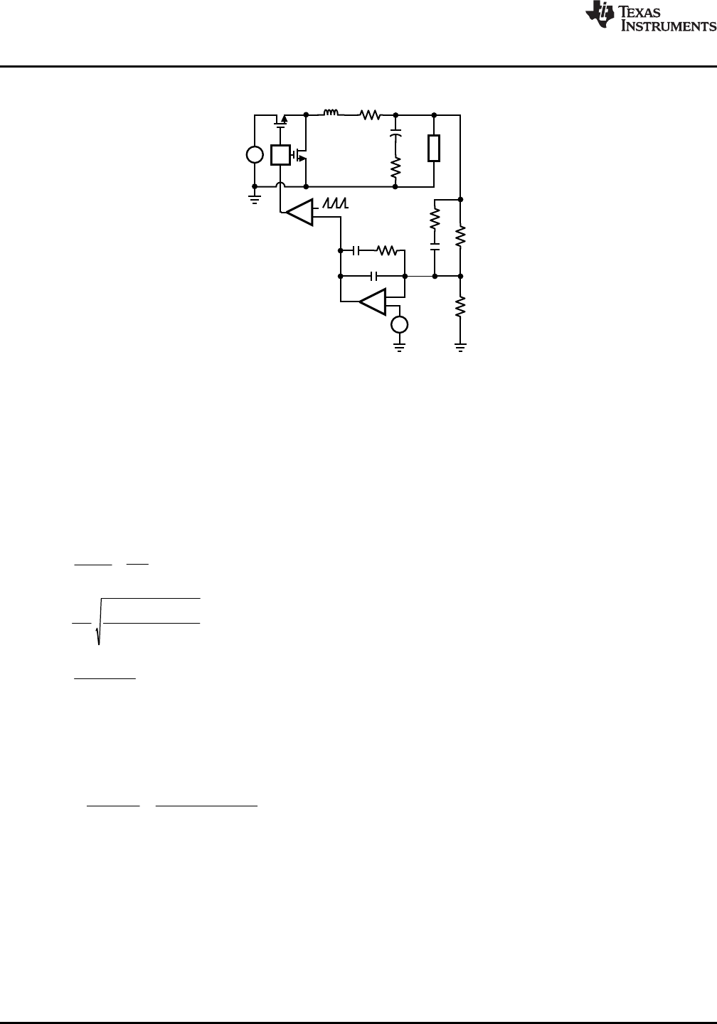
Figure 35. Power Stage and Error Amp
One popular method for selecting the compensation components is to create Bode plots of gain and phase for
the power stage and error amplifier. Combined, they make the overall bandwidth and phase margin of the
regulator easy to see. Software tools such as Excel, MathCAD, and Matlab are useful for showing how changes
in compensation or the power stage affect system gain and phase.
The power stage modulator provides a DC gain A
DC
that is equal to the input voltage divided by the peak-to-peak
value of the PWM ramp. This ramp is 1.0VP-P for the LM2743. The inductor and output capacitor create a
double pole at frequency f
DP
, and the capacitor ESR and capacitance create a single zero at frequency f
ESR
. For
this example, with V
IN
= 3.3V, these quantities are:
In the equation for f
DP
, the variable R
L
is the power stage resistance, and represents the inductor DCR plus the
on resistance of the top power MOSFET. R
O
is the output voltage divided by output current. The power stage
transfer function G
PS
is given by the following equation, and Figure 36 shows Bode plots of the phase and gain in
this example.
a = LC
O
(R
O
+ R
C
)
b = L + C
O
(R
O
R
L
+ R
O
R
C
+ R
C
R
L
)
c = R
O
+ R
L
22 Submit Documentation Feedback Copyright © 2004–2013, Texas Instruments Incorporated
Product Folder Links: LM2743