
Datasheet


Table Of Contents
- Features
- Applications
- Description
- Absolute Maximum Ratings
- Operating Ratings
- Electrical Characteristics
- Typical Performance Characteristics
- Block Diagram
- Application Information
- Revision History
+
BOOT
HG
LG
V
IN
V
O
V
CC
+
LM2743
D1
D2D3
+
LG
HG
BOOT
+
V
IN
D1
C
BOOT
LM2743
LM78L05
5V
V
O
V
CC
LM2743
www.ti.com
SNVS276G –APRIL 2004–REVISED MARCH 2013
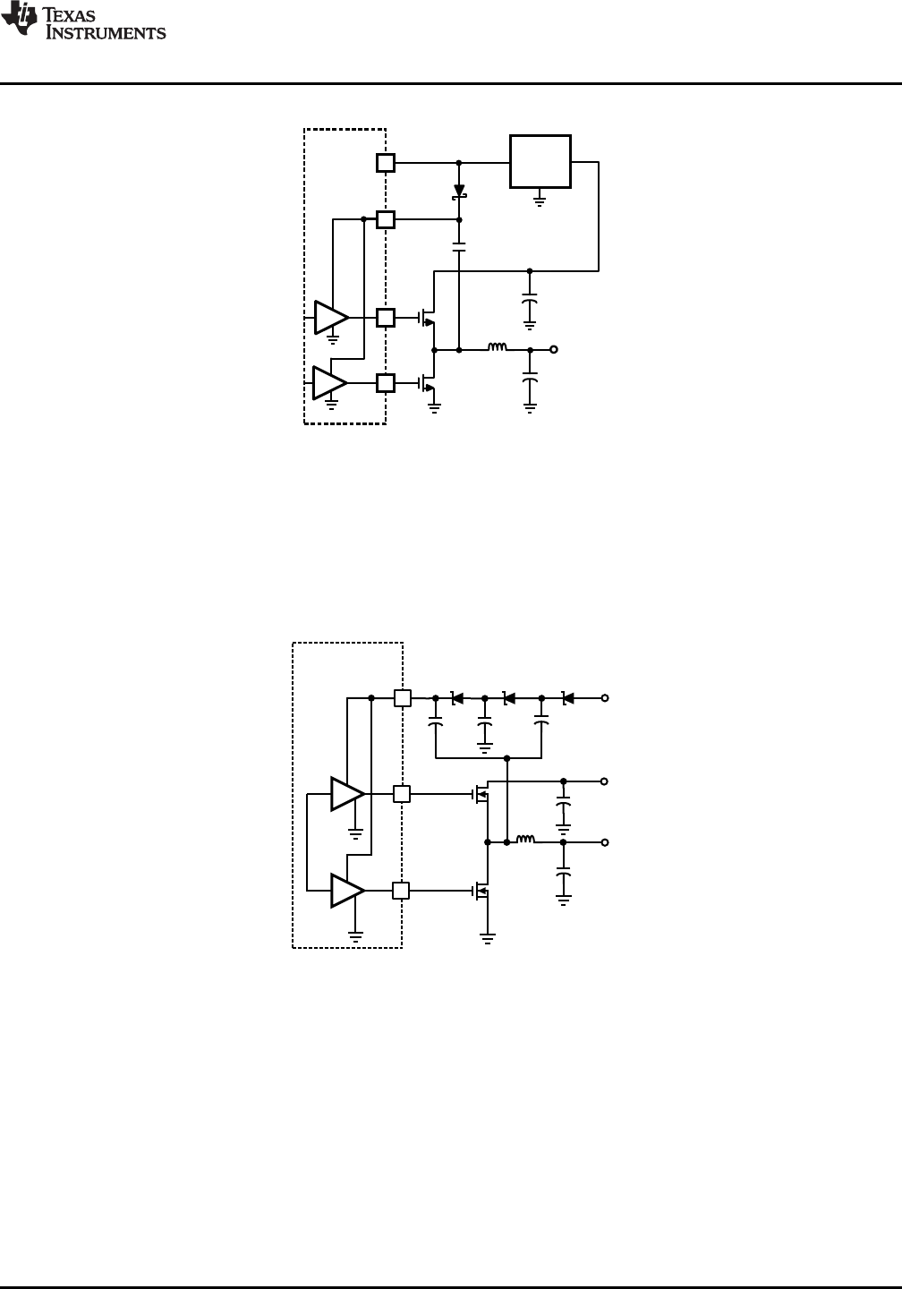
Figure 30. LM78L05 Feeding Basic Charge Pump
Figure 31 shows a second possibility for bootstrapping the MOSFET drives using a doubler. This circuit provides
an equal voltage drive of V
CC
- 3V
D
+ V
IN
to both the high-side and low-side MOSFET drives. This method should
only be used in circuits that use 3.3V for both V
CC
and V
IN
. Even with V
IN
= V
CC
= 3.0V (10% lower tolerance on
3.3V) and V
D
= 0.5V both high-side and low-side gates will have at least 4.5V of drive. The power dissipation of
the gate drive circuitry is directly proportional to gate drive voltage, hence the thermal limits of the LM2743 IC will
quickly be reached if this circuit is used with V
CC
or V
IN
voltages over 5V.
Figure 31. Charge Pump with Added Gate Drive
All the gate drive circuits shown in the above figures typically use 100 nF ceramic capacitors in the bootstrap
locations.
POWER GOOD SIGNAL
The open drain output on the Power Good pin needs a pull-up resistor to a low voltage source. The pull-up
resistor should be chosen so that the current going into the Power Good pin is less than 1 mA. A 100 kΩ resistor
is recommended for most applications.
Copyright © 2004–2013, Texas Instruments Incorporated Submit Documentation Feedback 15
Product Folder Links: LM2743