
Datasheet


Table Of Contents
- Features
- Applications
- Description
- Absolute Maximum Ratings
- Operating Ratings
- Electrical Characteristics
- Typical Performance Characteristics
- Block Diagram
- Application Information
- Revision History
+
BOOT
HG
LG
V
IN
V
O
V
CC
+
LM2743
D1
C
BOOT
LM2743
SNVS276G –APRIL 2004–REVISED MARCH 2013
www.ti.com
MOSFET GATE DRIVERS
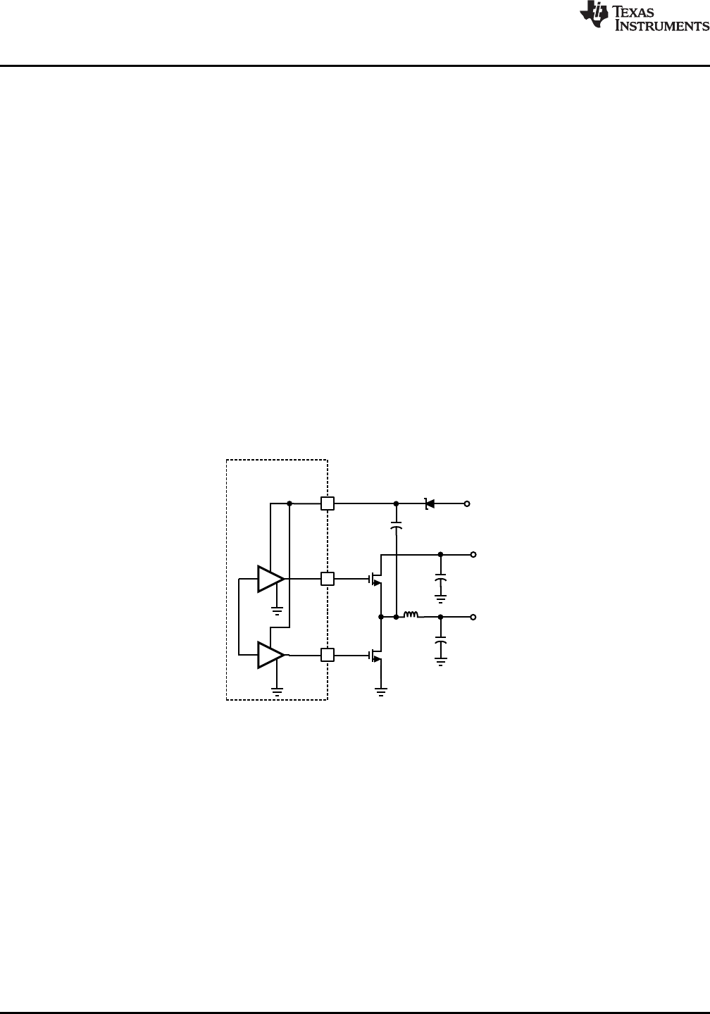
The LM2743 has two gate drivers designed for driving N-channel MOSFETs in a synchronous mode. Note that
unlike most other synchronous controllers, the bootstrap capacitor of the LM2743 provides power not only to the
driver of the upper MOSFET, but the lower MOSFET driver too (both drivers are ground referenced, i.e. no
floating driver). To fully turn the top MOSFET on, the BOOT voltage must be at least one gate threshold greater
than V
IN
when the high-side drive goes high. This bootstrap voltage is usually supplied from a local charge pump
structure. But looking at the Typical Application schematic, this also means that the difference voltage V
CC
- V
D1
,
which is the voltage the bootstrap capacitor charges up to, must be always greater than the maximum tolerance
limit of the threshold voltage of the upper MOSFET. Here V
D1
is the forward voltage drop across the bootstrap
diode D1. This therefore may place restrictions on the minimum input voltage and/or type of MOSFET used.
The most basic charge bootstrap pump circuit can be built using one Schottky diode and a small capacitor, as
shown in Figure 29. The capacitor C
BOOT
serves to maintain enough voltage between the top MOSFET gate and
source to control the device even when the top MOSFET is on and its source has risen up to the input voltage
level. The charge pump circuitry is fed from V
CC
, which can operate over a range from 3.0V to 6.0V. Using this
basic method the voltage applied to the gates of both high-side and low-side MOSFETs is V
CC
- V
D
. This method
works well when V
CC
is 5V±10%, because the gate drives will get at least 4.0V of drive voltage during the worst
case of V
CC-MIN
= 4.5V and V
D-MAX
= 0.5V. Logic level MOSFETs generally specify their on-resistance at V
GS
=
4.5V. When V
CC
= 3.3V±10%, the gate drive at worst case could go as low as 2.5V. Logic level MOSFETs are
not specified to turn on, or may have much higher on-resistance at 2.5V. Sub-logic level MOSFETs, usually
specified at V
GS
= 2.5V, will work, but are more expensive, and tend to have higher on-resistance. The circuit in
Figure 29 works well for input voltages ranging from 1V up to 16V and V
CC
= 5V ±10%, because the drive
voltage depends only on V
CC
.
Figure 29. Basic Charge Pump (Bootstrap)
Note that the LM2743 can be paired with a low cost linear regulator like the LM78L05 to run from a single input
rail between 6.0 and 14V. The 5V output of the linear regulator powers both the V
CC
and the bootstrap circuit,
providing efficient drive for logic level MOSFETs. An example of this circuit is shown in Figure 30.
14 Submit Documentation Feedback Copyright © 2004–2013, Texas Instruments Incorporated
Product Folder Links: LM2743