
Datasheet


Table Of Contents
LM2642
www.ti.com
SNVS203I –MAY 2002–REVISED APRIL 2013
ELECTRICAL CHARACTERISTICS
Unless otherwise specified, V
IN
= 15V, GND = PGND = 0V, VLIN5 = VDD1 = VDD2. Limits appearing in boldface type apply
over the specified operating junction temperature range, (-20°C to +125°C, if not otherwise specified). Specifications
appearing in plain type are measured using low duty cycle pulse testing with T
A
= 25°C
(1)
,
(2)
. Min/Max limits are specified by
design, test, or statistical analysis.
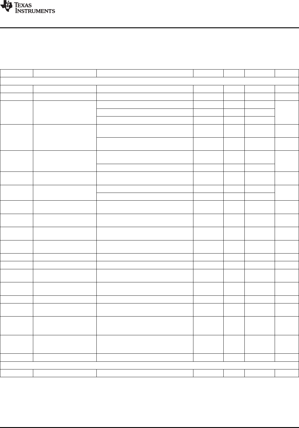
Symbol Parameter Conditions Min Typ Max Units
System
ΔV
OUT
/V
OUT
Load Regulation VIN = 15V, V
compx
= 0.5V to 1.5V 0.04 %
ΔV
OUT
/V
OUT
Line Regulation 5.5V ≤ VIN ≤ 30V, V
compx
=1.25V 0.04 %
V
FB1_FI2
Feedback Voltage 5.5V ≤ VIN ≤ 30V 1.215 1.238 1.260
0°C to 125°C 1.217 1.259 V
-40°C to 125°C 1.212 1.261
I
VIN
Input Supply Current V
ON_SSx
> 2V 1.0
mA
5.5V ≤ VIN ≤ 30V 2.0
Shutdown
(3)
37 µA
V
ON_SS1
= V
ON_SS2
= 0V 110
VLIN5 VLIN5 Output Voltage
(4)
IVLIN5 = 0 to 25mA,
4.70 5 5.30
5.5V ≤ VIN ≤ 30V
V
-40°C to 125°C 4.68 5.30
V
CLos
Current Limit Comparator
±2 ±7.0 mV
Offset (VILIMX −VRSNSX)
I
CL
Current Limit Sink Current 9 10 11
µA
-40°C to 125°C 8.67 11
I
ss_SC1
, Soft-Start Source Current V
ON_ss1
= V
ON_ss2
= 1.5V (on)
0.5 2 5.0 µA
I
ss_SC2
I
ss_SK1
, Soft-Start Sink Current V
ON_ss1
= V
ON_ss2
= 2V
2 5.2 10 µA
I
ss_SK2
V
ON_SS1
, Soft-Start On Threshold
0.7 1.12 1.4 V
V
ON_SS2
V
SSTO
Soft-Start Timeout
(5)
3.3 V
Threshold
I
sc_uvdelay
UV_DELAY Source Current UV-DELAY = 2V 2 5 9 µA
I
sk_uvdelay
UV_DELAY Sink Current UV-DELAY = 0.4V 0.2 0.48 1.2 mA
V
UVDelay
UV_DELAY Threshold
2.3 V
Voltage
V
UVP
FB1, FB2, Under Voltage As a percentage of nominal output voltage
75 80 86 %
Protection Latch Threshold (falling edge)
Hysteresis 4 %
V
OVP
V
OUT
Overvoltage As a percentage measured at V
FB1
, V
FB2
107 113 122 %
Shutdown Latch Threshold
V
pwrbad
Regulator Window Detector As a percentage of output voltage
Thresholds (PGOOD1 from 86.5 90.3 94.5 %
High to Low)
V
pwrgd
Regulator Window Detector
Thresholds (PGOOD1 from 91.5 94 97.0 %
Low to High)
S
wx_R
SW1, SW2 ON-Resistance V
SW1
= V
SW2
= 2V 420 480 535 Ω
Gate Drive
I
CBOOT
CBOOTx Leakage Current V
CBOOT1
= V
CBOOT2
= 7V 10 nA
(1) A typical is the center of characterization data measured with low duty cycle pulse tsting at T
A
= 25°C. Typicals are not ensured.
(2) All limits are specified. All electrical characteristics having room-temperature limits are tested during production with T
A
= T
J
= 25°C. All
hot and cold limits are specified by correlating the electrical characteristics to process and temperature variations and applying statistical
process control.
(3) Both switching controllers are off. The linear regulator VLIN5 remains on.
(4) The output voltage at the VLIN5 pin may be as high as 5.9V in shutdown mode (ON/SS1 = ON/SS2 = 0V).
(5) When SS1 and SS2 pins are charged above this voltage and either of the output voltages at Vout1 or Vout2 is still below the regulation
limit, the under voltage protection feature is initialized.
Copyright © 2002–2013, Texas Instruments Incorporated Submit Documentation Feedback 5
Product Folder Links: LM2642