
Datasheet


Table Of Contents
LM2642
www.ti.com
SNVS203I –MAY 2002–REVISED APRIL 2013
(18)
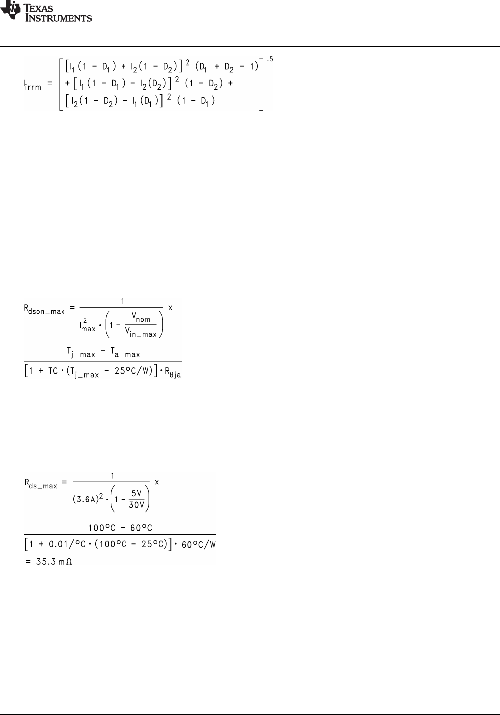
Where, again, I1 and I2 are the maximum load currents of channel 1 and 2, and D1 and D2 are the duty cycles.
This equation should be used when both duty cycles are expected to be higher than 50%.
Input capacitors must meet the minimum requirements of voltage and ripple current capacity. The size of the
capacitor should then be selected based on hold up time requirements. Bench testing for individual applications
is still the best way to determine a reliable input capacitor value. The input capacitor should always be placed as
close as possible to the current sense resistor or the drain of the top FET.
MOSFET SELECTION
BOTTOM FET SELECTION
During normal operation, the bottom FET is switching on and off at almost zero voltage. Therefore, only
conduction losses are present in the bottom FET. The most important parameter when selecting the bottom FET
is the on resistance (Rdson). The lower the on resistance, the lower the power loss. The bottom FET power loss
peaks at maximum input voltage and load current. The equation for the maximum allowed on resistance at room
temperature for a given FET package, is:
(19)
where Tj_max is the maximum allowed junction temperature in the FET, Ta_max is the maximum ambient
temperature, R
θja
is the junction-to-ambient thermal resistance of the FET, and TC is the temperature coefficient
of the on resistance which is typically in the range of 10,000ppm/°C.
If the calculated Rdson_max is smaller than the lowest value available, multiple FETs can be used in parallel.
This effectively reduces the Imax term in the above equation, thus reducing Rdson. When using two FETs in
parallel, multiply the calculated Rdson_max by 4 to obtain the Rdson_max for each FET. In the case of three
FETs, multiply by 9.
(20)
If the selected FET has an Rds value higher than 35.3Ω, then two FETs with an Rdson less than 141mΩ (4 x
35.3mΩ) can be used in parallel. In this case, the temperature rise on each FET will not go to Tj_max because
each FET is now dissipating only half of the total power.
TOP FET SELECTION
The top FET has two types of losses: switching loss and conduction loss. The switching losses mainly consist of
crossover loss and bottom diode reverse recovery loss. Since it is rather difficult to estimate the switching loss, a
general starting point is to allot 60% of the top FET thermal capacity to switching losses. The best way to
precisely determine switching losses is through bench testing. The equation for calculating the on resistance of
the top FET is thus:
Copyright © 2002–2013, Texas Instruments Incorporated Submit Documentation Feedback 21
Product Folder Links: LM2642