
Datasheet


Table Of Contents
LM2642
www.ti.com
SNVS203I –MAY 2002–REVISED APRIL 2013
Where ±δ% is the output voltage regulation window and ±ε% is the output voltage initial accuracy.
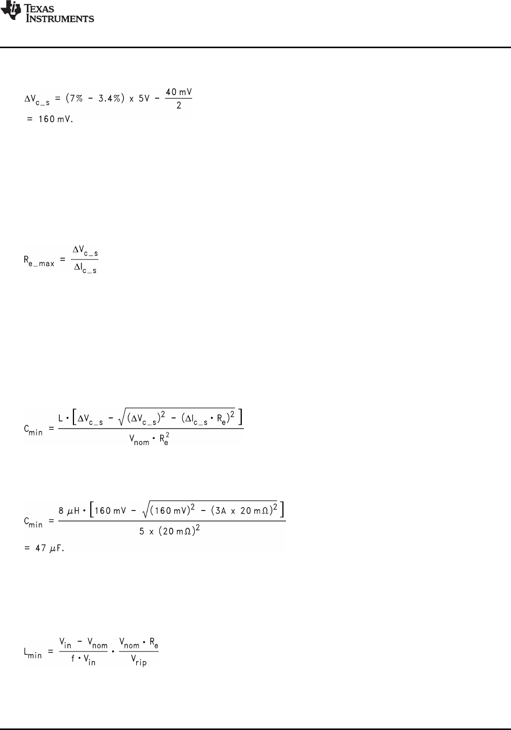
Example: Vnom = 5V, δ% = 7%, ε% = 3.4%, Vrip = 40mV peak to peak.
(8)
Since the ripple voltage is included in the calculation of ΔVc_s, the inductor ripple current should not be included
in the worst-case load current excursion. That is, the worst-case load current excursion should be simply
maximum load current change specification, ΔIc_s.
MAXIMUM ESR CALCULATION
Unless the rise and fall times of a load transient are slower than the response speed of the control loop, if the
total combined ESR (Re) is too high, the load transient requirement will not be met, no matter how large the
capacitance.
The maximum allowed total combined ESR is:
(9)
Example: ΔVc_s = 160mV, ΔIc_s = 3A. Then Re_max = 53.3mΩ.
Maximum ESR criterion can be used when the associated capacitance is high enough, otherwise more
capacitors than the number determined by this criterion should be used in parallel.
MINIMUM CAPACITANCE CALCULATION
In a switch mode power supply, the minimum output capacitance is typically dictated by the load transient
requirement. If there is not enough capacitance, the output voltage excursion will exceed the maximum allowed
value even if the maximum ESR requirement is met. The worst-case load transient is an unloading transient that
happens when the input voltage is the highest and when the present switching cycle has just finished. The
corresponding minimum capacitance is calculated as follows:
(10)
Notice it is already assumed the total ESR, Re, is no greater than Re_max, otherwise the term under the square
root will be a negative value. Also, it is assumed that L has already been selected, therefore the minimum L
value should be calculated before Cmin and after Re (see Inductor Selection below). Example: Re = 20mΩ,
Vnom = 5V, ΔVc_s = 160mV, ΔIc_s = 3A, L = 8µH
(11)
Generally speaking, Cmin decreases with decreasing Re, ΔIc_s, and L, but with increasing Vnom and ΔVc_s.
INDUCTOR SELECTION
The size of the output inductor can be determined from the desired output ripple voltage, Vrip, and the
impedance of the output capacitors at the switching frequency. The equation to determine the minimum
inductance value is as follows:
(12)
In the above equation, Re is used in place of the impedance of the output capacitors. This is because in most
cases, the impedance of the output capacitors at the switching frequency is very close to Re. In the case of
ceramic capacitors, replace Re with the true impedance.
Example: Vin (max)= 30V, Vnom = 5.0V, Vrip = 40mV, Re =20mΩ, f = 300kHz
Copyright © 2002–2013, Texas Instruments Incorporated Submit Documentation Feedback 19
Product Folder Links: LM2642