
Datasheet


Table Of Contents
V
IN
V
OUT
0 2 4 6 8 10 12 14 16 18 2022 24 26 28 30
0
5
10
15
20
25
30
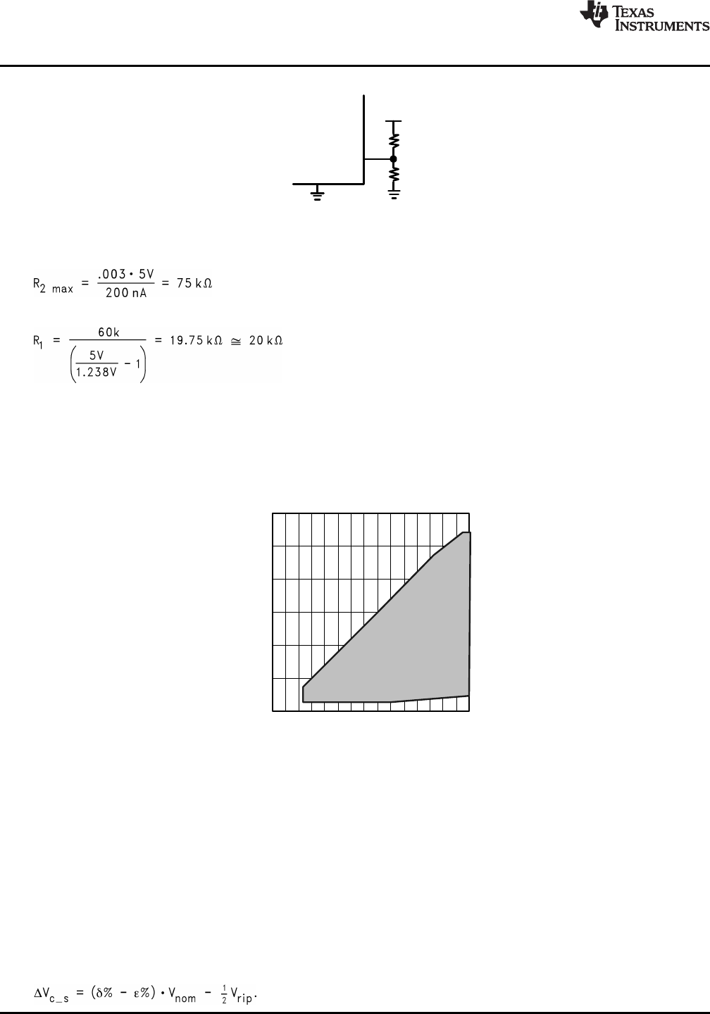
Vout
R2
FBx
GND
R1
LM2642
SNVS203I –MAY 2002–REVISED APRIL 2013
www.ti.com
Figure 27. Output Voltage Setting
Example: Vnom=5V, Vfb=1.238V, Ifbmax=200nA.
(5)
Choose 60K
(6)
The output voltage is limited by the maximum duty cycle as well as the minimum on time. Figure 28 shows the
limits for input and output voltages. The recommended maximum output voltage is approximately 1V less than
the nominal input voltage. At 30V input, the minimum output is approximately 2.3V and the maximum is
approximately 27V.
For input voltages below 5.5V, VLIN5 must be connected to Vin through a small resistor (approximately 4.7
ohm). This will ensure that VLIN5 does not fall below the UVLO threshold.
Figure 28. Available Output Voltage Range
OUTPUT CAPACITOR SELECTION
In applications that exhibit large and fast load current swings, the slew rate of such a load current transient may
be beyond the response speed of the regulator. Therefore, to meet voltage transient requirements during worst-
case load transients, special consideration should be given to output capacitor selection. The total combined
ESR of the output capacitors must be lower than a certain value, while the total capacitance must be greater
than a certain value. Also, in applications where the specification of output voltage regulation is tight and ripple
voltage must be low, starting from the required output voltage ripple will often result in fewer design iterations.
ALLOWED TRANSIENT VOLTAGE EXCURSION
The allowed output voltage excursion during a load transient (ΔVc_s) is:
(7)
18 Submit Documentation Feedback Copyright © 2002–2013, Texas Instruments Incorporated
Product Folder Links: LM2642