
Datasheet


Table Of Contents
FBx
1.13BG
in: 0.94BG
out: 0.91BG
in: 0.84BG
out: 0.80BG
OFF 1
UVPG1
UVP ½ (latched)
OVP ½ (latched)
ONx
SS Timeout
SD
power on
reset
shutdown
latch UVP
HDRV: off
LDRV: off
shutdown
latch OVP
HDRV: off
LDRV: on
TSD
UVLO
PGOOD1
OVP 1/2
UV_DELAY
5 µA
fault
from other CH.
OVPx
UVPGx
UVPx
from other CH.
_
+
_
+
_
+
OVP & PG
UVPG
UVP
PGOOD Protection
Comparators
LM2642
SNVS203I –MAY 2002–REVISED APRIL 2013
www.ti.com
SEQUENTIAL STARTUP
Sequential startup can be implemented by simply connecting PGOOD1 to SS/ON2. Once channel 1 has reached
94% of nominal, PGOOD1 will go high, thus enabling SS/ON2. In this mode of operation, channel 2 will be
controlled by the state of channel 1. If channel 1 falls out of the PGOOD1 window, channel 2 will be switched off
immediately.
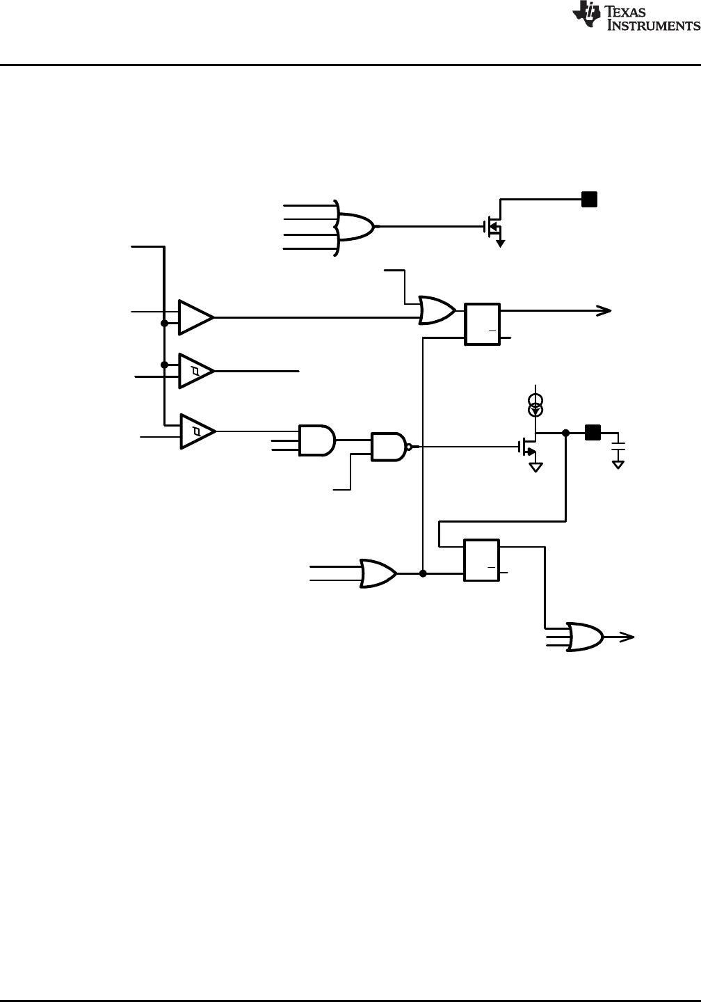
Figure 24. PGOOD, OVP and UVP
OVER VOLTAGE PROTECTION (OVP)
If the output voltage on either channel rises above 113% of nominal, over voltage protection activates. Both
channels will latch off, and the PGOOD1 pin will go low. When the OVP latch is set, the high side FET driver,
HDRVx, is immediately turned off and the low side FET driver, LDRVx, is turned on to discharge the output
capacitor through the inductor. To reset the OVP latch, either the input voltage must be cycled, or both channels
must be switched off.
UNDER VOLTAGE PROTECTION (UVP) AND UV DELAY
If the output voltage on either channel falls below 80% of nominal, under voltage protection activates. As shown
in Figure 24, an under-voltage event will shut off the UV_DELAY MOSFET, which will allow the UV_DELAY
capacitor to charge at 5uA (typical). At the UV_DELAY threshold (2.3V typical) both channels will latch off. Also,
UV_DELAY will be disabled and the UV_DELAY pin will return to 0V. During UVP, both the high side and low
side FET drivers will be turned off. If no capacitor is connected to the UV_DELAY pin, the UVP latch will be
activated immediately. To reset the UVP latch, either the input voltage must be cycled, or both ON/SS pins must
be pulled low. The UVP function can be disabled by connecting the UV_DELAY pin to ground.
14 Submit Documentation Feedback Copyright © 2002–2013, Texas Instruments Incorporated
Product Folder Links: LM2642