
Datasheet


Table Of Contents
- Features
- Applications
- Description
- Absolute Maximum Ratings
- Operating Conditions
- LM2596-3.3 Electrical Characteristics
- LM2596-5.0 Electrical Characteristics
- LM2596-12 Electrical Characteristics
- LM2596-ADJ Electrical Characteristics
- All Output Voltage Versions Electrical Characteristics
- Typical Performance Characteristics
- Test Circuit and Layout Guidelines
- Application Information
- EXTERNAL COMPONENTS
- FEEDFORWARD CAPACITOR (Adjustable Output Voltage Version)
- OUTPUT CAPACITOR
- CATCH DIODE
- INDUCTOR SELECTION
- DISCONTINUOUS MODE OPERATION
- OUTPUT VOLTAGE RIPPLE AND TRANSIENTS
- OPEN CORE INDUCTORS
- THERMAL CONSIDERATIONS
- DELAYED STARTUP
- UNDERVOLTAGE LOCKOUT
- INVERTING REGULATOR
- INVERTING REGULATOR SHUTDOWN METHODS
- Revision History
LM2596
SNVS124C –NOVEMBER 1999–REVISED APRIL 2013
www.ti.com
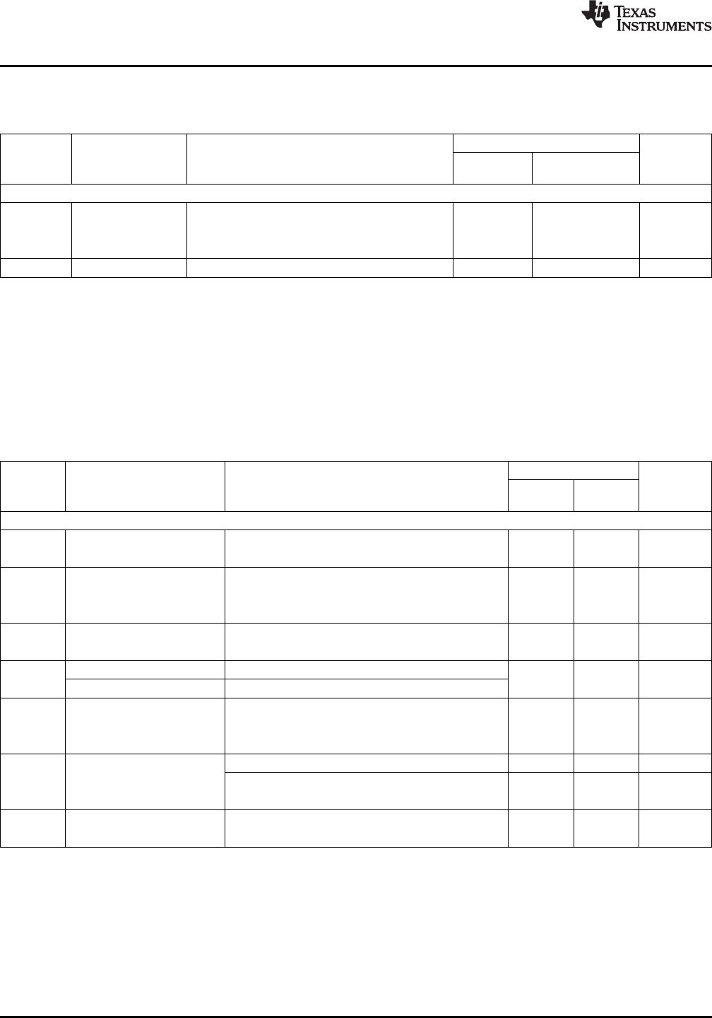
LM2596-ADJ Electrical Characteristics
Specifications with standard type face are for T
J
= 25°C, and those with boldface type apply over full Operating
Temperature Range
LM2596-ADJ
Units
Symbol Parameter Conditions
Typ Limit
(Limits)
(1) (2)
SYSTEM PARAMETERS
(3)
Test Circuit Figure 20
V
FB
Feedback Voltage 4.5V ≤ V
IN
≤ 40V, 0.2A ≤ I
LOAD
≤ 3A 1.230 V
V
OUT
programmed for 3V. Circuit of Figure 20 1.193/1.180 V(min)
1.267/1.280 V(max)
η Efficiency V
IN
= 12V, V
OUT
= 3V, I
LOAD
= 3A 73 %
(1) Typical numbers are at 25°C and represent the most likely norm.
(2) All limits specified at room temperature (standard type face) and at temperature extremes (bold type face). All room temperature limits
are 100% production tested. All limits at temperature extremes are ensured via correlation using standard Statistical Quality Control
(SQC) methods. All limits are used to calculate Average Outgoing Quality Level (AOQL).
(3) External components such as the catch diode, inductor, input and output capacitors, and voltage programming resistors can affect
switching regulator system performance. When the LM2596 is used as shown in the Figure 20 test circuit, system performance will be
as shown in system parameters of Electrical Characteristics section.
All Output Voltage Versions Electrical Characteristics
Specifications with standard type face are for T
J
= 25°C, and those with boldface type apply over full Operating
Temperature Range. Unless otherwise specified, V
IN
= 12V for the 3.3V, 5V, and Adjustable version and V
IN
= 24V for the
12V version. I
LOAD
= 500 mA
LM2596-XX
Units
Symbol Parameter Conditions
Typ Limit
(Limits)
(1) (2)
DEVICE PARAMETERS
I
b
Feedback Bias Current Adjustable Version Only, V
FB
= 1.3V 10 nA
50/100 nA (max)
f
O
Oscillator Frequency See
(3)
150 kHz
127/110 kHz(min)
173/173 kHz(max)
V
SAT
Saturation Voltage I
OUT
= 3A
(4) (5)
1.16 V
1.4/1.5 V(max)
DC Max Duty Cycle (ON) See
(5)
100 %
Min Duty Cycle (OFF) See
(6)
0
I
CL
Current Limit Peak Current
(4)(5)
4.5 A
3.6/3.4 A(min)
6.9/7.5 A(max)
I
L
Output Leakage Current Output = 0V
(4)(6)
50 μA(max)
Output = −1V
(7)
2 mA
30 mA(max)
I
Q
Quiescent Current See
(6)
5 mA
10 mA(max)
(1) Typical numbers are at 25°C and represent the most likely norm.
(2) All limits specified at room temperature (standard type face) and at temperature extremes (bold type face). All room temperature limits
are 100% production tested. All limits at temperature extremes are ensured via correlation using standard Statistical Quality Control
(SQC) methods. All limits are used to calculate Average Outgoing Quality Level (AOQL).
(3) The switching frequency is reduced when the second stage current limit is activated.
(4) No diode, inductor or capacitor connected to output pin.
(5) Feedback pin removed from output and connected to 0V to force the output transistor switch ON.
(6) Feedback pin removed from output and connected to 12V for the 3.3V, 5V, and the ADJ. version, and 15V for the 12V version, to force
the output transistor switch OFF.
(7) V
IN
= 40V.
4 Submit Documentation Feedback Copyright © 1999–2013, Texas Instruments Incorporated
Product Folder Links: LM2596