
Datasheet


PCB Layout
www.ti.com
12 PCB Layout
The PCB was manufactured with 2oz. copper outer layers, and 1oz. copper inner layers. Twenty 8 mil.
diameter vias placed underneath the device, along with addional vias placed throughout the ground plane
around the device, help improve the thermal dissipation of the board.
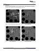
Figure 11. Top Layer (Copper planes outlined in grey) Figure 12. Mid Layer1
Figure 13. Mid Layer2 Figure 14. Bottom Layer
12
AN-2176 LM10010 Evaluation Board SNVA498B–July 2011–Revised May 2013
Submit Documentation Feedback
Copyright © 2011–2013, Texas Instruments Incorporated