
Datasheet


Write to
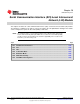
SPIDAT
VCLK
SPISCS
SPICLK
SPISIMO
SPISOMI
* Dotted vertical lines indicate the receive edges
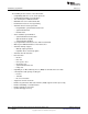
VCLK
Write to
SPIDAT
SPICLK
SPISIMO
SPISOMI
* Dotted vertical lines indicate the receive edges
MibSPI Pin Timing Parameters
www.ti.com
27.6 MibSPI Pin Timing Parameters
The pin timings of SPI can be classified based on its mode of operation. In each mode, different
configurations like Phase & Polarity affect the pin timings.
The pin directions are based on the mode of operation.
Master mode SPI:
• SPICLK (SPI Clock) - Output
• SPISIMO (SPI Slave In Master Out) - Output
• SPISCS[7:0] (SPI Slave Chip Selects) - Output
• SPISOMI (SPI Slave Out Master In) - Input
• SPIENA (SPI slave ready Enable) - Input
Slave mode SPI:
• SPICLK - Input
• SPISIMO - Input
• SPISCS - Input
• SPISOMI - Output
• SPIENA - Output
NOTE: All the following timing diagrams are with Phase = 0 and Polarity = 0, unless explicitly stated
otherwise.
27.6.1 Master Mode Timings for SPI/MibSPI
Figure 27-93. SPI/MibSPI Pins During Master Mode 3-Pin Configuration
Figure 27-94. SPI/MibSPI Pins During Master Mode 4-Pin with SPISCS Configuation
1338
Multi-Buffered Serial Peripheral Interface Module (MibSPI) with Parallel Pin SPNU562–May 2014
Option (MibSPIP)
Submit Documentation Feedback
Copyright © 2014, Texas Instruments Incorporated