
Datasheet


Table Of Contents
- 1 Device Overview
- Table of Contents
- 2 Revision History
- 3 Device Comparison
- 4 Terminal Configuration and Functions
- 4.1 PGE QFP Package Pinout (144-Pin)
- 4.2 ZWT BGA Package Ball-Map (337 Ball Grid Array)
- 4.3 Terminal Functions
- 4.3.1 PGE Package
- 4.3.1.1 Multibuffered Analog-to-Digital Converters (MibADC)
- 4.3.1.2 Enhanced High-End Timer Modules (N2HET)
- 4.3.1.3 Enhanced Capture Modules (eCAP)
- 4.3.1.4 Enhanced Quadrature Encoder Pulse Modules (eQEP)
- 4.3.1.5 Enhanced Pulse-Width Modulator Modules (ePWM)
- 4.3.1.6 General-Purpose Input / Output (GPIO)
- 4.3.1.7 Controller Area Network Controllers (DCAN)
- 4.3.1.8 Local Interconnect Network Interface Module (LIN)
- 4.3.1.9 Standard Serial Communication Interface (SCI)
- 4.3.1.10 Inter-Integrated Circuit Interface Module (I2C)
- 4.3.1.11 Standard Serial Peripheral Interface (SPI)
- 4.3.1.12 Multibuffered Serial Peripheral Interface Modules (MibSPI)
- 4.3.1.13 Ethernet Controller
- 4.3.1.14 USB Host and Device Port Controller Interface
- 4.3.1.15 System Module Interface
- 4.3.1.16 Clock Inputs and Outputs
- 4.3.1.17 Test and Debug Modules Interface
- 4.3.1.18 Flash Supply and Test Pads
- 4.3.1.19 Supply for Core Logic: 1.2V nominal
- 4.3.1.20 Supply for I/O Cells: 3.3V nominal
- 4.3.1.21 Ground Reference for All Supplies Except VCCAD
- 4.3.2 ZWT Package
- 4.3.2.1 Multibuffered Analog-to-Digital Converters (MibADC)
- 4.3.2.2 Enhanced High-End Timer Modules (N2HET)
- 4.3.2.3 Enhanced Capture Modules (eCAP)
- 4.3.2.4 Enhanced Quadrature Encoder Pulse Modules (eQEP)
- 4.3.2.5 Enhanced Pulse-Width Modulator Modules (ePWM)
- 4.3.2.6 General-Purpose Input / Output (GPIO)
- 4.3.2.7 Controller Area Network Controllers (DCAN)
- 4.3.2.8 Local Interconnect Network Interface Module (LIN)
- 4.3.2.9 Standard Serial Communication Interface (SCI)
- 4.3.2.10 Inter-Integrated Circuit Interface Module (I2C)
- 4.3.2.11 Standard Serial Peripheral Interface (SPI)
- 4.3.2.12 Multibuffered Serial Peripheral Interface Modules (MibSPI)
- 4.3.2.13 Ethernet Controller
- 4.3.2.14 USB Host and Device Port Controller Interface
- 4.3.2.15 External Memory Interface (EMIF)
- 4.3.2.16 System Module Interface
- 4.3.2.17 Clock Inputs and Outputs
- 4.3.2.18 Test and Debug Modules Interface
- 4.3.2.19 Flash Supply and Test Pads
- 4.3.2.20 Reserved
- 4.3.2.21 No Connects
- 4.3.2.22 Supply for Core Logic: 1.2V nominal
- 4.3.2.23 Supply for I/O Cells: 3.3V nominal
- 4.3.2.24 Ground Reference for All Supplies Except VCCAD
- 4.3.1 PGE Package
- 5 Specifications
- 5.1 Absolute Maximum Ratings Over Operating Free-Air Temperature Range
- 5.2 ESD Ratings
- 5.3 Power-On Hours (POH)
- 5.4 Device Recommended Operating Conditions
- 5.5 Switching Characteristics Over Recommended Operating Conditions for Clock Domains
- 5.6 Wait States Required
- 5.7 Power Consumption Over Recommended Operating Conditions
- 5.8 Input/Output Electrical Characteristics Over Recommended Operating Conditions
- 5.9 Thermal Resistance Characteristics
- 5.10 Output Buffer Drive Strengths
- 5.11 Input Timings
- 5.12 Output Timings
- 5.13 Low-EMI Output Buffers
- 6 System Information and Electrical Specifications
- 6.1 Device Power Domains
- 6.2 Voltage Monitor Characteristics
- 6.3 Power Sequencing and Power On Reset
- 6.4 Warm Reset (nRST)
- 6.5 ARM Cortex-R4F CPU Information
- 6.6 Clocks
- 6.7 Clock Monitoring
- 6.8 Glitch Filters
- 6.9 Device Memory Map
- 6.10 Flash Memory
- 6.11 Tightly Coupled RAM Interface Module
- 6.12 Parity Protection for Accesses to Peripheral RAMs
- 6.13 On-Chip SRAM Initialization and Testing
- 6.14 External Memory Interface (EMIF)
- 6.15 Vectored Interrupt Manager
- 6.16 DMA Controller
- 6.17 Real Time Interrupt Module
- 6.18 Error Signaling Module
- 6.19 Reset / Abort / Error Sources
- 6.20 Digital Windowed Watchdog
- 6.21 Debug Subsystem
- 7 Peripheral Information and Electrical Specifications
- 7.1 Enhanced Translator PWM Modules (ePWM)
- 7.1.1 ePWM Clocking and Reset
- 7.1.2 Synchronization of ePWMx Time Base Counters
- 7.1.3 Synchronizing all ePWM Modules to the N2HET1 Module Time Base
- 7.1.4 Phase-Locking the Time-Base Clocks of Multiple ePWM Modules
- 7.1.5 ePWM Synchronization with External Devices
- 7.1.6 ePWM Trip Zones
- 7.1.7 Triggering of ADC Start of Conversion Using ePWMx SOCA and SOCB Outputs
- 7.1.8 Enhanced Translator-Pulse Width Modulator (ePWMx) Timings
- 7.2 Enhanced Capture Modules (eCAP)
- 7.3 Enhanced Quadrature Encoder (eQEP)
- 7.4 Multibuffered 12bit Analog-to-Digital Converter
- 7.5 General-Purpose Input/Output
- 7.6 Enhanced High-End Timer (N2HET)
- 7.7 Controller Area Network (DCAN)
- 7.8 Local Interconnect Network Interface (LIN)
- 7.9 Serial Communication Interface (SCI)
- 7.10 Inter-Integrated Circuit (I2C)
- 7.11 Multibuffered / Standard Serial Peripheral Interface
- 7.12 Ethernet Media Access Controller
- 7.13 Universal Serial Bus (USB) Host and Device Controllers
- 7.1 Enhanced Translator PWM Modules (ePWM)
- 8 Device and Documentation Support
- 9 Mechanical Packaging and Orderable Information
- Important Notice
- 1518515_DS2.pdf
310
310
RTICLK
310
310
310
External
control
CAP eventsource0
CAP eventsource1
=
Upcounter
Capture
upcounter
Compare
upcounter
Freerunningcounter
Capture
RTIFRCx
freerunningcounter
RTICAFRCx
OVLINTx
RTICPUCx
RTIUCx
RTICAUCx
ToCompare
Unit
NTU0
NTU1
NTU2
NTU3
RM46L852
SPNS185C –SEPTEMBER 2012 –REVISED JUNE 2015
www.ti.com
6.17 Real Time Interrupt Module
The real-time interrupt (RTI) module provides timer functionality for operating systems and for
benchmarking code. The RTI module can incorporate several counters that define the timebases needed
for scheduling an operating system.
The timers also allow you to benchmark certain areas of code by reading the values of the counters at the
beginning and the end of the desired code range and calculating the difference between the values.
6.17.1 Features
The RTI module has the following features:
• Two independent 64 bit counter blocks
• Four configurable compares for generating operating system ticks or DMA requests. Each event can
be driven by either counter block 0 or counter block 1.
• Fast enabling/disabling of events
• Two time-stamp (capture) functions for system or peripheral interrupts, one for each counter block
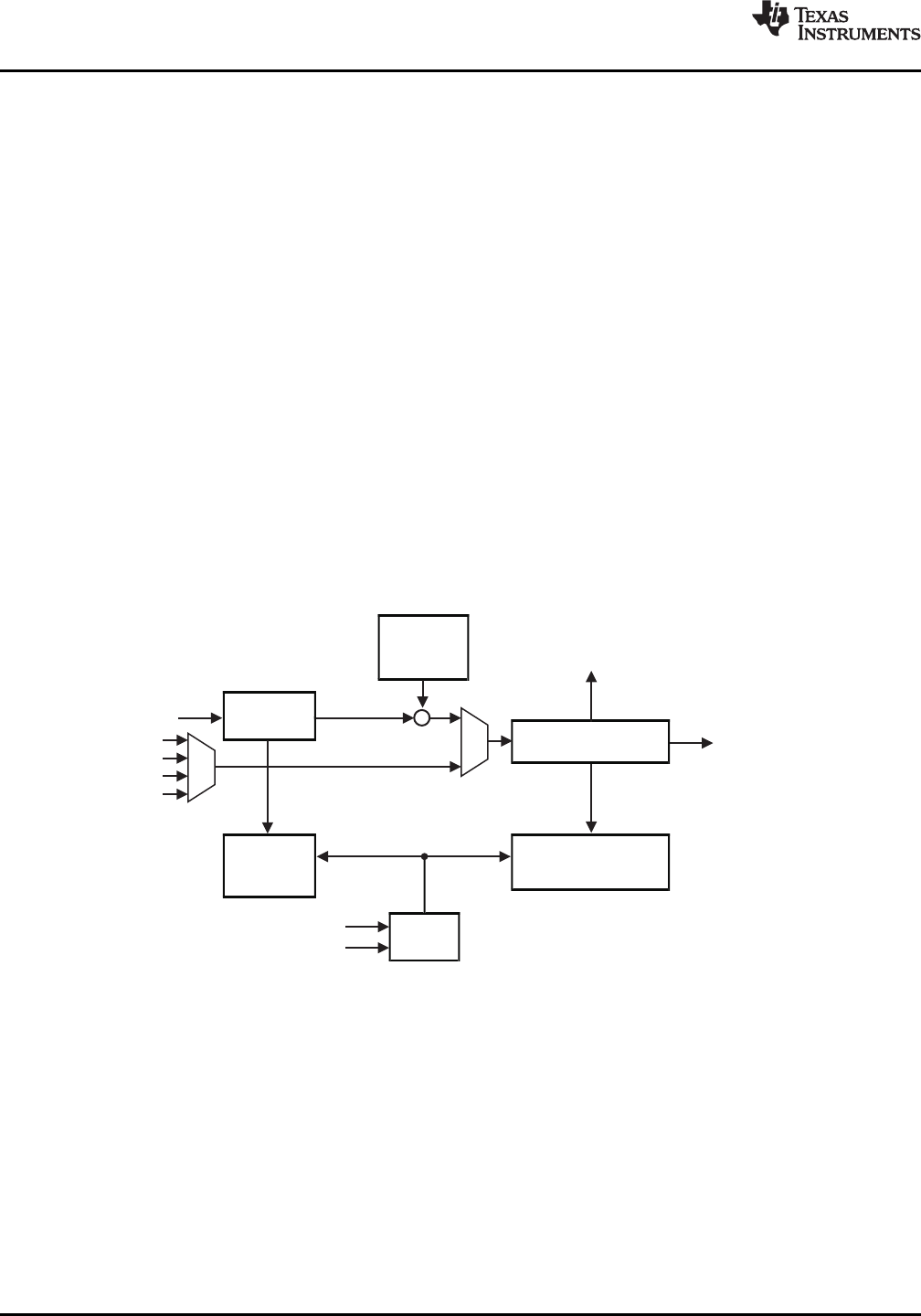
6.17.2 Block Diagrams
Figure 6-18 shows a high-level block diagram for one of the two 64-bit counter blocks inside the RTI
module. Both the counter blocks are identical except the Network Time Unit (NTUx) inputs are only
available as time base inputs for the counter block 0.
Figure 6-18. Counter Block Diagram
110 System Information and Electrical Specifications Copyright © 2012–2015, Texas Instruments Incorporated
Submit Documentation Feedback
Product Folder Links: RM46L852