
Datasheet


V+ > 3 V
I
L
I A2 0, INA 1N 7 27
74HC04
A1
A2
Single-Pole Filter
Capacitor
5 kW
5 kW
96 kW
R
L
PRE OUT
BUF IN
GND
IN–IN+ V+
Load
−16 V to +80 V
Supply
R
S
0.01 µF
OUT
Negative
and Positive
Common-Mode
Voltage
INA270-Q1, INA271-Q1
SBOS401B –JULY 2007–REVISED FEBRUARY 2010
www.ti.com
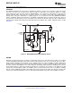
Shutdown
The INA270 and INA271 do not provide a shutdown pin; however, because they consume a quiescent current
less than 1 mA, they can be powered by either the output of logic gates or by transistor switches to supply
power. Driving the gate low shuts down the INA270/INA271. Use a totem-pole output buffer or gate that can
provide sufficient drive along with 0.1-mF bypass capacitor, preferably ceramic with good high-frequency
characteristics. This gate should have a supply voltage of 3 V or greater, because the INA270 and INA271
require a minimum supply greater than 2.7 V. In addition to eliminating quiescent current, this gate also turns off
the 10-mA bias current present at each of the inputs. Note that the IN+ and IN– inputs are able to withstand full
common-mode voltage under all powered and under-powered conditions. An example shutdown circuit is shown
in Figure 5.
Figure 5. INA270/INA271 Example Shutdown Circuit
RFI/EMI
Attention to good layout practices is always recommended. Keep traces short and, when possible, use a printed
circuit board (PCB) ground plane with surface-mount components placed as close to the device pins as possible.
Small ceramic capacitors placed directly across amplifier inputs can reduce RFI/EMI sensitivity. PCB layout
should locate the amplifier as far away as possible from RFI sources. Sources can include other components in
the same system as the amplifier itself, such as inductors (particularly switched inductors handling a lot of current
and at high frequencies). RFI can generally be identified as a variation in offset voltage or dc signal levels with
changes in the interfering RF signal. If the amplifier cannot be located away from sources of radiation, shielding
may be needed. Twisting wire input leads makes them more resistant to RF fields. The difference in input pin
location of the INA270 and INA271 versus the INA193 through INA198 may provide different EMI performance.
12 Submit Documentation Feedback Copyright © 2007–2010, Texas Instruments Incorporated
Product Folder Link(s): INA270-Q1 INA271-Q1