
Datasheet


V
OUT
(V)
V
SENSE
(mV)
0.40
0.36
0.32
0.28
0.24
0.20
0.16
0.12
0.08
0.04
0
0 202 6 8 10 12 14 184 16
Actual
Ideal
0.48
0.48
0.40
0.36
0.32
0.28
0.24
0.20
0.16
0.12
0.08
0.04
0
0
2
4 6 8 10 12 14 16 18 20 22
V
OUT
(V)
V
SENSE
(mV)
24
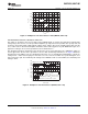
INA271 V
OUT
Limit
(1)
V
CM2
V
CM1
V
CM3
V
CM4
V
CM2
, V
CM3
, and V
CM4
illustrate the variance
from part to part of the V
CM
that can cause
maximum V
OUT
with V
SENSE
< 20mV.
V
OUT
limit at V
SENSE
= 0mV,
0
≤
V
CM1
≤
V
S
Ideal
INA270-Q1, INA271-Q1
www.ti.com
SBOS401B –JULY 2007–REVISED FEBRUARY 2010
Figure 3. Example for Low V
SENSE
Cases 1 and 3 (INA271, Gain = 20)
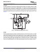
Low V
SENSE
Case 2: V
SENSE
< 20 mV, 0 V ≤ V
CM
≤ V
S
This region of operation is the least accurate for the INA270 family. To achieve the wide input common-mode
voltage range, these devices use two operational amplifier (op amp) front ends in parallel. One op amp front end
operates in the positive input common-mode voltage range, and the other in the negative input region. For this
case, neither of these two internal amplifiers dominates and overall loop gain is very low. Within this region, V
OUT
approaches voltages close to linear operation levels for Normal Case 2.
This deviation from linear operation becomes greatest the closer V
SENSE
approaches 0 V. Within this region, as
V
SENSE
approaches 20 mV, device operation is closer to that described by Normal Case 2. Figure 4 illustrates
this behavior for the INA271. The V
OUT
maximum peak for this case is determined by maintaining a constant V
S
,
setting V
SENSE
= 0 mV and sweeping V
CM
from 0 V to V
S
. The exact V
CM
at which V
OUT
peaks during this case
varies from part to part. The maximum peak voltage for the INA270 is 0.28 V; for the INA271, the maximum peak
voltage is 0.4 V.
Figure 4. Example for Low V
SENSE
Case 2 (INA271, Gain = 20)
Copyright © 2007–2010, Texas Instruments Incorporated Submit Documentation Feedback 11
Product Folder Link(s): INA270-Q1 INA271-Q1