
Datasheet


Table Of Contents
INA148-Q1
www.ti.com
SBOS472A –MARCH 2009–REVISED OCTOBER 2011
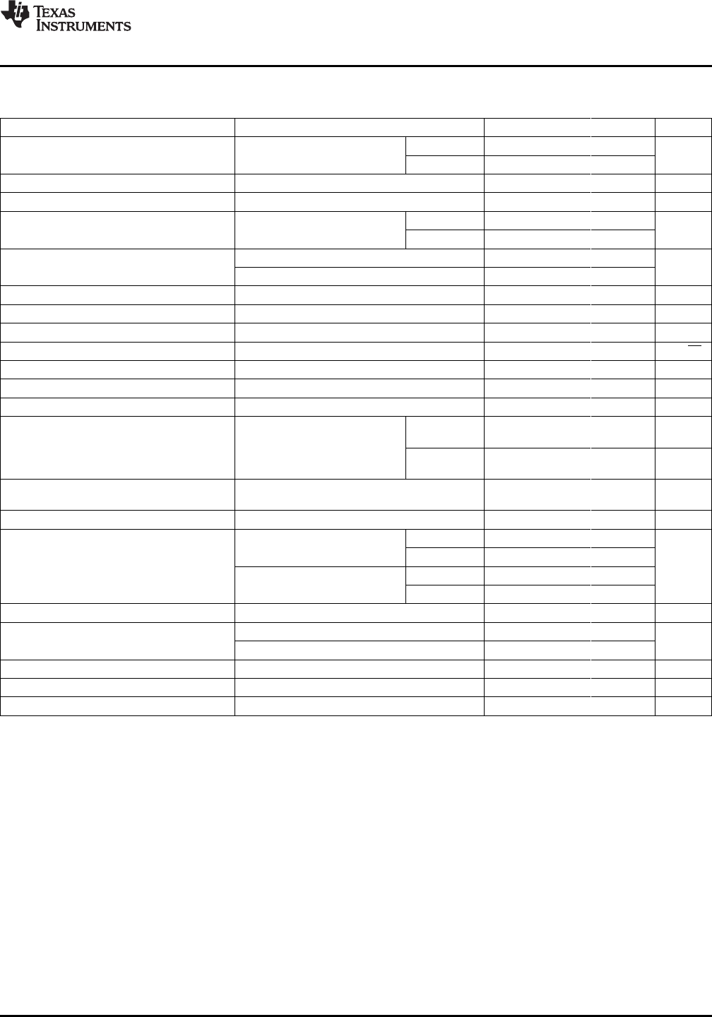
ELECTRICAL CHARACTERISTICS
V
S
= ±5 V to ±15 V (dual supply), R
L
= 10 kΩ to ground, V
REF
= 0 V, T
A
= 25°C (unless otherwise noted)
PARAMETER TEST CONDITIONS MIN TYP MAX UNIT
V
S
= ±15 V ±1 ±5
V
OS
Input offset voltage
(1) (2)
V
CM
= 0 V mV
V
S
= ±5 V ±1 ±5
ΔV
OS
/ΔT Input offset voltage drift
(1)
T
A
= –40°C to 125°C ±10 μV/°C
PSRR Power supply ripple rejection
(1)
V
S
= ±1.35 V to ±18 V, V
CM
= 0 V ±50 ±400 μV/V
V
S
= ±15 V –200 200
V
CM
Common-mode voltage range V
+IN
– V
–IN
= 0 V
V
S
= ±5 V –100 80
V
S
= ±15 V, V
CM
= –200 V to 200 V, R
S
= 0 Ω 70 86
CMRR Common-mode rejection ratio dB
V
S
= ±5 V, V
CM
= –100 V to 80 V, R
S
= 0 Ω 70 86
Differential input impedance 2 MΩ
Common-mode input impedance 1 MΩ
V
n
Voltage noise
(1) (3)
f = 0.1 Hz to 10 Hz 17 μV
p-p
Voltage noise density
(1) (3)
f = 1 kHz 880 nV/√Hz
Initial gain
(1)
1 V/V
Gain error V
O
= (V– + 0.5) to (V+ – 1.5) ±0.01 ±0.075 %
Gain error over temperature ±3 ±10 ppm/°C
±0.00
V
S
= ±15 V ±0.002 %FSR
1
Gain nonlinearity V
O
= (V– + 0.5) to (V+ – 1.5)
±0.00
V
S
= ±5 V %FSR
1
Small signal bandwidth frequency
100 kHz
response
SR Slew rate 1 V/μs
0.1% 21
V
S
= ±15 V, 10-V step
0.01% 25
t
s
Settling time μs
0.1% 21
V
S
= ±5 V, 6-V step
0.01% 25
Overload recovery 50% input overload 24 μs
R
L
= 100 kΩ V– + 0.25 V+ – 1
V
O
Output voltage V
R
L
= 10 kΩ V– + 0.5 V+ – 1.5
I
O
Output current Short-circuit current, continuous to common ±13 mA
C
L
Load capacitance Stable operation 10 nF
I
S
Supply current V
IN
= 0, I
O
= 0 ±260 ±300 μA
(1) Overall difference amplifier configuration. Referred to input pins (V
+IN
and V
–IN
), gain = 1 V/V.
(2) Includes effects of amplifier's input bias and offset currents.
(3) Includes effects of input current noise and thermal noise contribution of resistor network.
Copyright © 2009–2011, Texas Instruments Incorporated Submit Documentation Feedback 3
Product Folder Link(s): INA148-Q1