
Datasheet


Table Of Contents
1 MW 50 kW
52.6316 kW
50 kW
2.7778 kW
1 MW
7
3
2
6
4
1
A1
INA148
–15 V
V
O
+15 V
±15-mV Offset Trim Range, RTI
100 kW
100 kW
100 W
+15 V
–15 V
V
REF
OPA237
V
+IN
V
–IN
V = (V – V )
O +IN –IN
1 MW 50 kW
52.6316 kW
50 kW
2.7778 kW
1 MWR
C
R
S
I
L
V
CM
7
3
200 V
2
6
4 1
A1
INA148
–15 V
V
O
+15 V
Load
V
O
= I
L
× R
S
Make R
C
= R
S
if R
S
100³ W
INA148-Q1
www.ti.com
SBOS472A –MARCH 2009–REVISED OCTOBER 2011
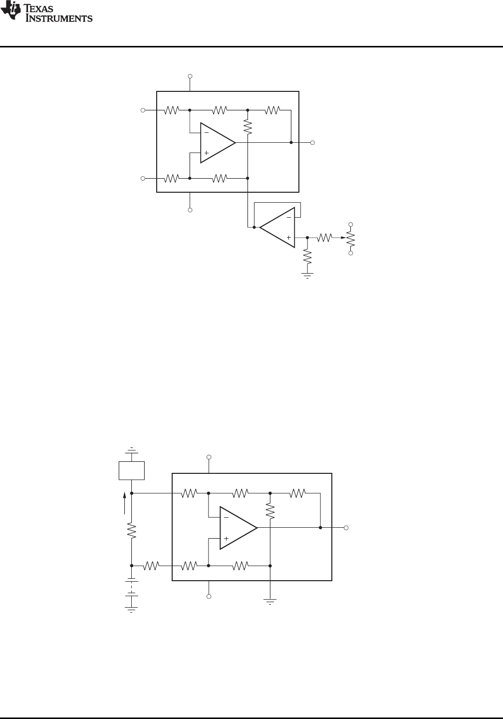
Figure 3. Preferred Offset Trim Circuit
Input Impedance
The input resistor network determines the impedance of each of the INA148 inputs. It is approximately 1 MΩ.
Unlike an instrumentation amplifier, signal source impedances at the two input terminals must be nearly equal to
maintain good common-mode rejection.
A mismatch between the two inputs' source impedances causes a differential amplifier's common-mode rejection
to be degraded. With a source impedance imbalance of only 500 Ω, CMR can fall to approximately 66 dB.
Figure 4 shows a common application—measuring power supply current through a shunt resistor (R
S
). A shunt
resistor creates an unbalanced source resistance condition that can degrade a differential amplifier's common
mode rejection.
Figure 4. Shunt-Resistor Current Measurement Circuit
Unless the shunt resistor is less than approximately 100 Ω, an additional equal compensating resistor (RC) is
recommended to maintain input balance and high CMR.
Copyright © 2009–2011, Texas Instruments Incorporated Submit Documentation Feedback 11
Product Folder Link(s): INA148-Q1