
Datasheet


Table Of Contents
1 MW 50 kW
52.6316 kW
50 kW
10 kW
10 kW
+15 V
–15 V
10 W
2.7778 kW
1 MW190 W
7
3
2
6
4 1
A1
INA148
–V
S
V
O
+V
S
±15-mV Offset Trim Range, RTI
V
REF
V
+IN
V
–IN
V = (V – V )
O +IN –IN
INA148-Q1
SBOS472A –MARCH 2009–REVISED OCTOBER 2011
www.ti.com
Common-Mode Range
The 20:1 input resistor ratio of the INA148 provides an input common-mode range that extends well beyond its
power supply rails.
The exact input voltage range depends on the amplifier's power-supply voltage and the voltage applied to the
REF terminal (pin 1). Typical input voltage ranges at different power supply voltages can be found in the
applications circuits section.
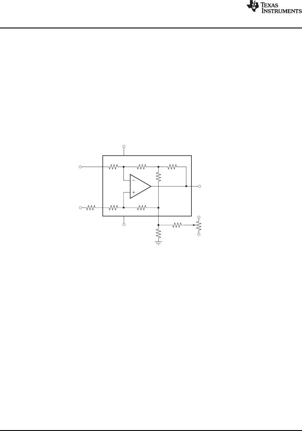
Offset Trim
The INA148 is laser-trimmed for low offset voltage and drift. Most applications require no external offset
adjustment.
Because a voltage applied to the reference (REF) pin (pin 1) is summed directly into the amplifier's output signal,
this technique can be used to null the amplifier's input offset voltage. Figure 2 shows an optional circuit for
trimming the offset voltage.
Figure 2. Optional Offset Trim Circuit
To maintain high common-mode rejection (CMR), the source impedance of any signal applied to the REF
terminal should be very low (≤5 Ω).
A source impedance of only 10 Ω at the REF pin reduces the INA148's CMR to approximately 74 dB. High CMR
can be restored if a resistor is added in series with the amplifier's positive input terminal (pin 3). This resistor
should be 19 times the source impedance that drives the REF pin. For example, if the REF pin sees a source
impedance of 10 Ω, a resistor of 190 Ω should be added in series with pin 3.
Preferably, the offset trim voltage applied to the REF pin should be buffered with an amplifier such as an
OPA237 (see Figure 3). In this case, the op amp output impedance is low enough that no external resistor is
needed to maintain the INA148's excellent CMR.
10 Submit Documentation Feedback Copyright © 2009–2011, Texas Instruments Incorporated
Product Folder Link(s): INA148-Q1