
User's Manual


MSP-TS430L092
www.ti.com
Settings of the MSP-TS430L092 Target Socket
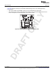
Figure B-6 shows the PCB layout of the MSP-TS430L092 target socket. The following pinning is
recommended:
• JP1 is write enable for the EPROM. If this is not set, the EPROM can only be read.
• JP2 and JP3 connect device supply with boost converter. They can be opened to measure device
current consumption. For default operation, they should be closed.
Figure B-6. MSP-TS430L092 Target Socket Module, PCB
40
Hardware SLAU278I–May 2009–Revised May 2012
Submit Documentation Feedback
Copyright © 2009–2012, Texas Instruments Incorporated