
Datasheet


DS92LX2122
(Top View)
1
2
3
4
5
6
7
8
9
10
11
12
13
14
15
16
17
18
19
20
21
22
23
24
36
35
34
33
32
31
30
29
28
27
26
25
48
47
46
45
44
43
42
41
40
39
38
37
ROUT[14]
ROUT[15]
ROUT[17]
ROUT[18]
ROUT[20]
PCLK
SCL
SDA
ROUT[3]
ROUT[2]
ROUT[0]
V
DDOR1
GPI[1]
GPI[0]
PDB
V
DDR
V
DDSSCG
ROUT[19]
V
DDOR3
ROUT[16] ROUT[1]
GPI[3]
GPI[2]
LOCK
ROUT[13]
ROUT[11]
ROUT[6]
ROUT[4]
ROUT[12]
ROUT[5]
ROUT[10]
V
DDD
ROUT[9]
M/S
RES
V
DDPLL
BISTEN
RES
RIN-
RIN+
V
DDCML
RES
RES
CAD
PASS
ROUT[8]
ROUT[7]
V
DDOR2
DAP = GND
DS92LX2121, DS92LX2122
SNLS330I –MAY 2010–REVISED APRIL 2013
www.ti.com
DS92LX2121 Serializer PIN DESCRIPTIONS (continued)
Pin Name Pin No. I/O, Type Description
CONTROL AND CONFIGURATION
Power down Mode Input Pin.
Input, LVCMOS w/ PDB = H, Transmitter is enabled and is ON.
PDB 13
pull down PDB = L, Transmitter is in Sleep (Power Down). When the transmitter is in the
SLEEP state, the PLL is shutdown, and IDD is minimized.
Input, LVCMOS w/ Reserved. This pin MUST be tied LOW.
RES 10, 11
pull down
Channel Link III INTERFACE
DOUT+ 17 Input/Output, CML Non-inverting differential output, back-channel input.
DOUT- 16 Input/Output, CML Inverting differential output, back-channel input.
Power and Ground
VDDPLL 14 Power, Analog PLL Power, 1.8V ±5%
VDDT 15 Power, Analog Tx Analog Power, 1.8V ±5%
VDDCML 18 Power, Analog LVDS & BC Dr Power, 1.8V ±5%
VDDD 34 Power, Digital Digital Power, 1.8V ±5%
VDDIO 31 Power, Digital Power for input stage, The single-ended inputs are powered from V
DDIO
.
Ground, DAP DAP must be grounded. Connect to the ground plane (GND) with at least 16
VSS DAP
vias.
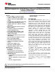
DS92LX2122 Pin Diagram
Top View
Figure 4. Deserializer - DS92LX2122
48-Pin WQFN (RHS Package)
4 Submit Documentation Feedback Copyright © 2010–2013, Texas Instruments Incorporated
Product Folder Links: DS92LX2121 DS92LX2122