
Datasheet


Table Of Contents
DS90C383B
www.ti.com
SNLS177G –APRIL 2004–REVISED APRIL 2013
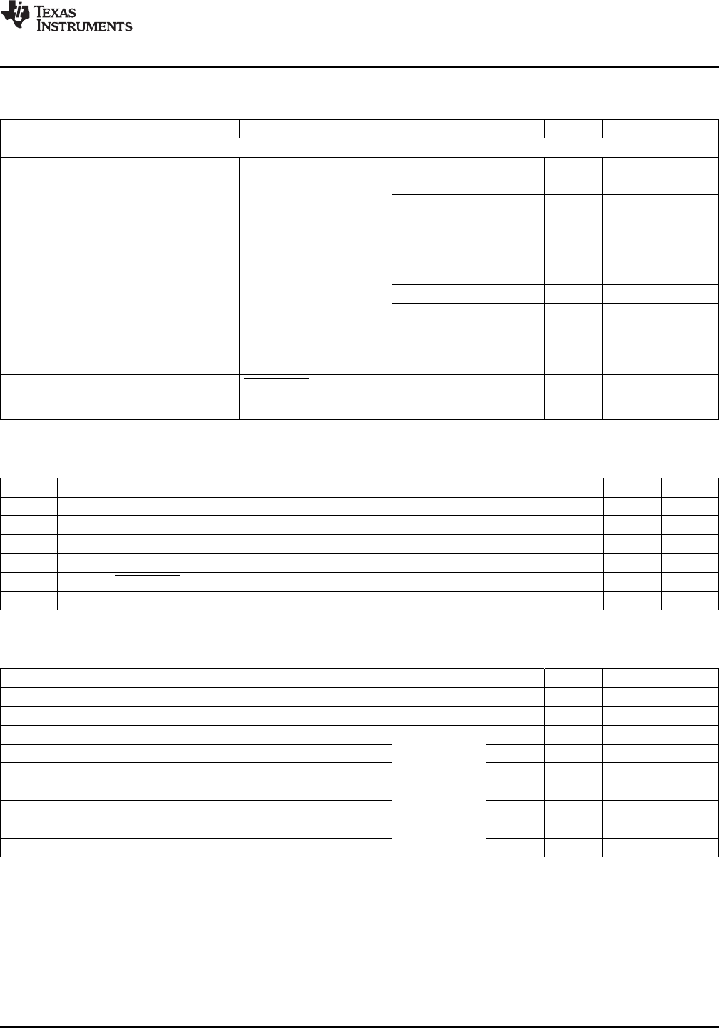
Electrical Characteristics
(1)
(continued)
Over recommended operating supply and temperature ranges unless otherwise specified.
Symbol Parameter Conditions Min Typ
(2)
Max Unit
TRANSMITTER SUPPLY CURRENT
ICCTW Transmitter Supply Current, R
L
= 100Ω, f = 25MHz 31 45 mA
Worst Case C
L
= 5 pF,
f = 40MHz 37 50 mA
Worst Case Pattern
f = 65 MHz 48 60 mA
(Figure 2 Figure 5) "Typ"
values are given for V
CC
=
3.6V and T
A
= +25°C, " Max
" values are given for V
CC
=
3.6V and T
A
= -10°C
ICCTG Transmitter Supply Current, R
L
= 100Ω, f = 25MHz 29 40 mA
16 Grayscale C
L
= 5 pF,
f = 40MHz 33 45 mA
16 Grayscale Pattern
f = 65 MHz 39 50 mA
(Figure 3 Figure 5) "Typ"
values are given for V
CC
=
3.6V and T
A
= +25°C, " Max
" values are given for V
CC
=
3.6V and T
A
= -10°C
ICCTZ Transmitter Supply Current, Power Down = Low 17 150 μA
Power Down Driver Outputs in TRI-STATE
®
under Power
Down Mode
Recommended Transmitter Input Characteristics
Over recommended operating supply and temperature ranges unless otherwise specified
Symbol Parameter Min Typ Max Unit
TCIT TxCLK IN Transition Time (Figure 6) 5 ns
TCIP TxCLK IN Period (Figure 7) 14.7 T 50 ns
TCIH TxCLK IN High Time (Figure 7) 0.35T 0.5T 0.65T ns
TCIL TxCLK IN Low Time (Figure 7) 0.35T 0.5T 0.65T ns
TXIT TxIN, and Power Down pins Transition Time 1.5 6.0 ns
TXPD Minimum pulse width for Power Down pin signal 1 us
Transmitter Switching Characteristics
Over recommended operating supply and temperature ranges unless otherwise specified
Symbol Parameter Min Typ Max Unit
LLHT LVDS Low-to-High Transition Time (Figure 5) 0.75 1.4 ns
LHLT LVDS High-to-Low Transition Time (Figure 5) 0.75 1.4 ns
TPPos0 Transmitter Output Pulse Position for Bit 0 (Figure 12)
(1)
f = 65 MHz -0.20 0 +0.20 ns
TPPos1 Transmitter Output Pulse Position for Bit 1 2.00 2.20 2.40 ns
TPPos2 Transmitter Output Pulse Position for Bit 2 4.20 4.40 4.60 ns
TPPos3 Transmitter Output Pulse Position for Bit 3 6.39 6.59 6.79 ns
TPPos4 Transmitter Output Pulse Position for Bit 4 8.59 8.79 8.99 ns
TPPos5 Transmitter Output Pulse Position for Bit 5 10.79 10.99 11.19 ns
TPPos6 Transmitter Output Pulse Position for Bit 6 12.99 13.19 13.39 ns
(1) The Minimum and Maximum Limits are based on statistical analysis of the device performance over process, voltage, and temperature
ranges. This parameter is functionality tested only on Automatic Test Equipment (ATE).
Copyright © 2004–2013, Texas Instruments Incorporated Submit Documentation Feedback 3
Product Folder Links: DS90C383B