
Datasheet


Table Of Contents
- FEATURES
- Applications
- DESCRIPTION
- Absolute Maximum Ratings
- Recommended Operating Conditions
- Electrical Characteristics
- Setup and Timing Diagrams
- Functional Description
- Application Information
- TYPICAL APPLICATION
- MULTIPLE HOP APPLICATION
- MATRIX SWITCH APPLICATION
- DUAL LINK APPLICATION
- DC AND AC COUPLED APPLICATIONS
- CABLE SELECTION AND INTER-PAIR SKEW
- 28 AWG STP (SHIELDED TWIST PAIRS) DVI / HDMI CABLES RECOMMENDED EQ SETTINGS
- 24 AWG UTP (LOW SKEW UNSHIELDED TWIST PAIRS) CABLES
- General Recommendations
- Typical Performance Characteristics as a Repeater
- Revision History
EQ0
EQ1
EQ2
DE0
DE1
SD
LOCK
VOD_CRL
LFp
LFn
GND
DAP
VDD
VDD
VDD
VDD
VDD
VDD
DS34RT5110
HDMI / DVI
Retimer
C_IN+
C_IN-
D_IN0+
C_OUT+
3V3
TMDS INPUT PORT - 4 CHANNEL
TMDS OUTPUT PORT - 4 CHANNEL
Input
Equalization
Control
10 PF
DC Couple 50 Ö Termination
PLL
EQ DE
EN
BYPASS
Reserv
3V3
All Bypass CAPS
0.1 PF unless noted.
10 PF
VDD
Output
De-E
Control
D_IN0-
D_IN1+
D_IN2+
D_IN1-
D_IN2-
C_OUT-
D_OUT0+
D_OUT0-
D_OUT2+
D_OUT1+
D_OUT1-
D_OUT2-
VDD
VDD
VDD
VDD
Other
Control
Analog
Pins
Other
Outputs
MODE
MODE
1
0
CDR
AVCC
AVCC
AVCC
AVCC
GND
t
SL
LOCK
SD
50%
50%
DS34RT5110
www.ti.com
SNLS310G –MARCH 2009–REVISED APRIL 2013
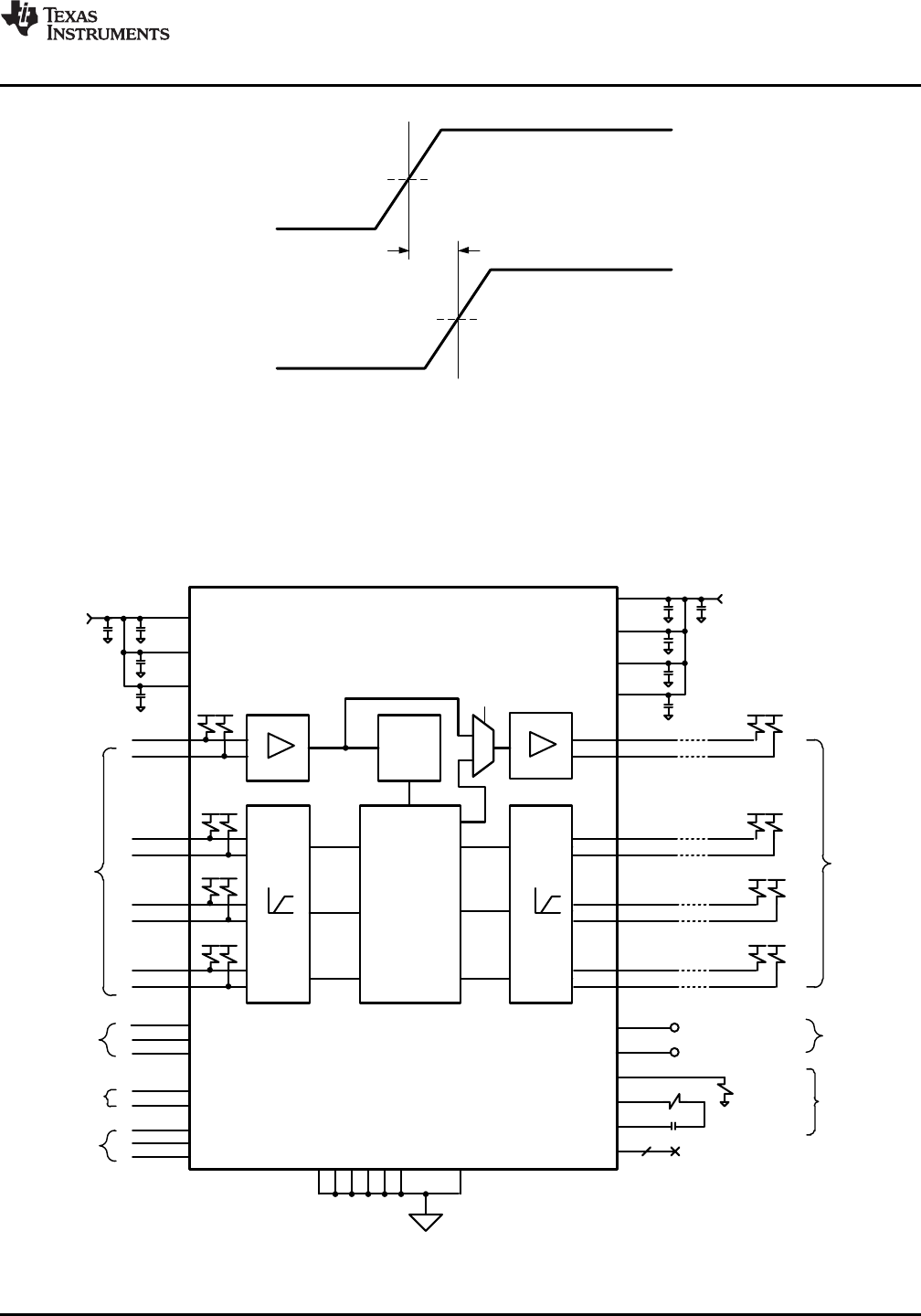
Figure 5. SD – LOCK Delay Time
Functional Description
The DS34RT5110 DVI, HDMI Retimer with Input Equalization and Output De-Emphasis consists of three data
channels and a clock channel. Each data channel consists of a TMDS compatible receiver with a power efficient
equalizer, a dedicated clock-data recovery (CDR) unit, and a TMDS compatible transmitter.
Figure 6. Block Diagram
Copyright © 2009–2013, Texas Instruments Incorporated Submit Documentation Feedback 9
Product Folder Links: DS34RT5110